CMOS (complementary metal oxide semiconductor) device for realizing global exposure, terminal thereof and exposure control method

A global exposure and terminal technology, applied to color TV components, TV system components, TVs, etc., can solve problems such as uneven exposure, poor user photography experience, and affecting the final imaging effect

Inactive Publication Date: 2016-09-28
NUBIA TECHNOLOGY CO LTD
View PDF9 Cites 1 Cited by
  • Summary
  • Abstract
  • Description
  • Claims
  • Application Information

AI Technical Summary

Problems solved by technology

[0003] Due to the mechanical structure of the mechanical shutter, there will be wear and tear in the process of opening and closing. Due to this wear, the mechanical shutter will have a limited service life. etc. In addition, because the mechanical shutter is controlled by the solenoid valve to close the mechanical blade, it takes a period of time from power-on to the complete closure of the solenoid valve suction blade, so when processing the mechanical shutter closing action, it is necessary to calculate the advance amount for operation, such as figure 1 As shown, it takes a period of time for the mechanical shutter to be completely closed (time T2) from being powered on (time T1), that is, as figure 1 As shown, in the CMOS global shutter exposure mode, after reaching the preset exposure time (T1 to T2 ...

Method used


Image

  • CMOS (complementary metal oxide semiconductor) device for realizing global exposure, terminal thereof and exposure control method
  • CMOS (complementary metal oxide semiconductor) device for realizing global exposure, terminal thereof and exposure control method
  • CMOS (complementary metal oxide semiconductor) device for realizing global exposure, terminal thereof and exposure control method

Examples


Embodiment 1

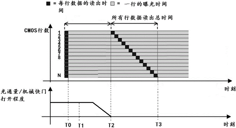
[0089] further reference Figure 4 , this embodiment proposes a CMOS device for realizing global exposure, the device includes: a complementary metal oxide semiconductor CMOS image sensor 300, a substrate 320 located below the CMOS image sensor, such as Figure 5 shown. Figure 4 The image pickup element 1212 in can be the CMOS image sensor.

[0090] like Figure 5 As shown, a layer of electronic thin film 310 is arranged between the CMOS image sensor 300 and the substrate 320, and the light projected from the CMOS image sensor 300 is incident on the substrate 320 after being transmitted through the electronic thin film 310, so that the light incident on the substrate 320 The amount of light on the light varies with the light transmission process.

[0091] According to the embodiment of the present invention, an electronic thin film is provided between the CMOS image sensor and the substrate, and the light transmittance of the electronic thin film is realized by controlling...

Embodiment 2

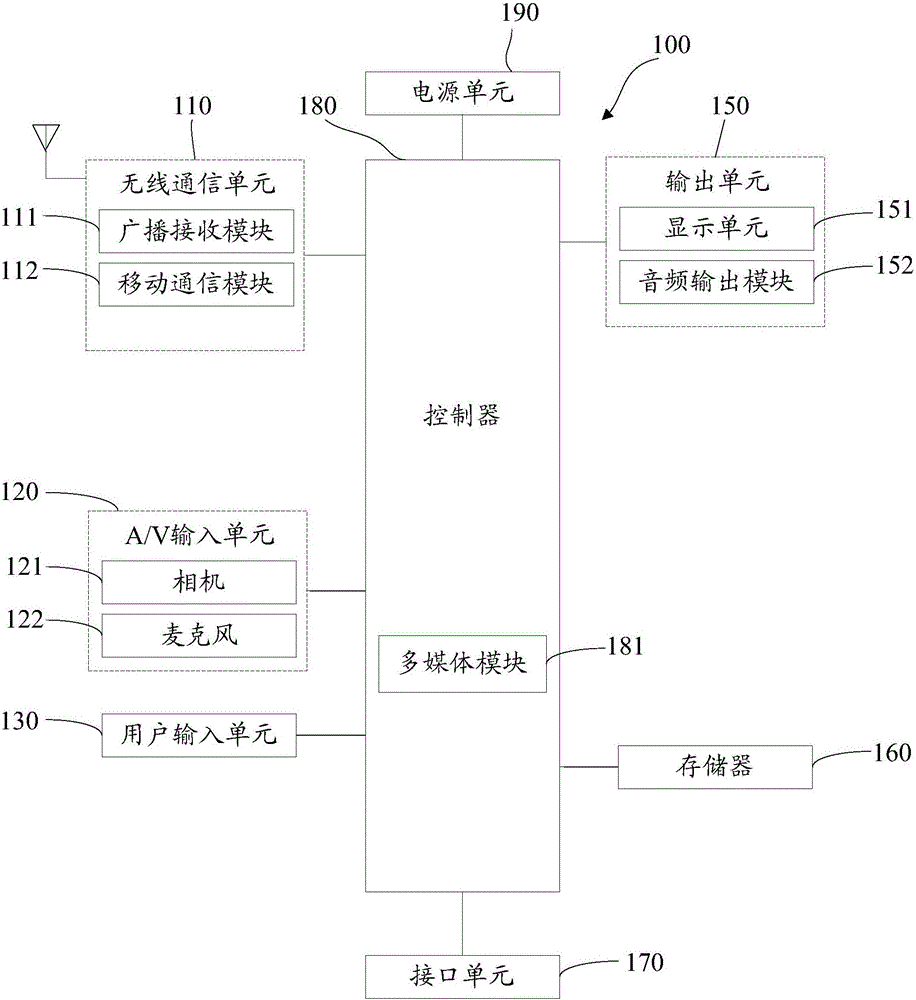
[0100] like Figure 7 as shown, Figure 7 It is a schematic diagram of functional modules of an embodiment of the terminal of the present invention. It should be emphasized that, for those skilled in the art, Figure 7 The shown functional block diagram is only an example diagram of a preferred embodiment, and those skilled in the art will Figure 7 The functional modules of the exposure device of the mobile terminal shown can be easily supplemented with new functional modules; the names of each functional module are self-defined names, which are only used to assist in understanding the various program function blocks of the exposure device of the mobile terminal. To limit the technical solution of the present invention, the core of the technical solution of the present invention is the functions to be achieved by the functional modules with respective self-defined names.

[0101] The terminal of the embodiment of the present invention, such as Figure 7 As shown, the term...

Embodiment 3

[0105] In the terminal of the embodiment of the present invention, the terminal includes: a memory and a processor; wherein, the memory contains computer-executable codes, which are used to implement the information mutual conversion method of the identification information in the above embodiment; the processor can pass The computer-executable code contained in the memory implements the scheme of mutual conversion of identification information.

[0106] The terminal may be an electronic device such as a PC, a portable electronic device such as a PAD, a tablet computer, or a laptop computer, or an intelligent mobile terminal such as a mobile phone, and is not limited to the description here. Wherein, for the processor, when performing processing, a microprocessor, a central processing unit (CPU, Central Processing Unit), a digital signal processor (DSP, Digital SingnalProcessor) or a programmable logic array ( FPGA, Field-Programm able Gate Array) to achieve.

[0107] An exam...


PUM


Abstract

The invention discloses a CMOS (complementary metal oxide semiconductor) device for realizing global exposure, a terminal thereof and an exposure control method. The CMOS device for realizing global exposure includes a complementary metal oxide semiconductor (CMOS) image sensor and a substrate below the CMOS image sensor; and an electronic film is arranged between the CMOS image sensor and the substrate, so that light emitted by the CMOS image sensor can be subjected to light transmitting processing of the electronic film, and then the processed light irradiates the substrate, and therefore, the amount of the light irradiating the substrate can be changed with the light transmitting processing.

Description

technical field [0001] The present invention relates to a CMOS (Complementary Metal-Oxide Semiconductor, Complementary Metal-Oxide Semiconductor) structure improvement technology, in particular to a CMOS device for realizing global exposure, its terminal, and an exposure control method. Background technique [0002] Many existing mobile terminals (such as mobile phones, etc.) use CMOS image sensors as lenses; and many CMOS image sensors use rolling shutter exposure mode (pixel point progressive exposure), in order to avoid Exposure) when taking pictures of high-speed moving objects, there will be a jelly effect, and the global shutter exposure mode (all pixels are exposed at the same time) is often used. However, due to the limitations of the design structure of most current CMOS image sensors, after exposure with the global shutter, need Read out the exposure data line by line for a period of time, such as figure 1 The period from T2 to T3 is the process of reading out row...

Claims


Application Information

Patent Timeline
IPC IPC(8): H04N5/374H04N5/378H04N5/235
CPCH04N23/73H04N25/76H04N25/75H04N25/77
Inventor 谢书勋
Owner NUBIA TECHNOLOGY CO LTD
Why Eureka
Try Eureka