Wafer test pattern yield loss calculation method

A calculation method, wafer testing technology, applied in the direction of semiconductor/solid-state device testing/measurement, etc., can solve the problems of biased judgment results, inability to calculate and analyze the loss rate of test patterns, and labor-intensive problems, so as to achieve the effect of reducing output

Active Publication Date: 2016-10-05
WINBOND ELECTRONICS CORP
View PDF4 Cites 3 Cited by
  • Summary
  • Abstract
  • Description
  • Claims
  • Application Information

AI Technical Summary

Problems solved by technology

[0003] However, most semiconductor factories still use manual identification to judge the test patterns in the wafer image. This is not only labor-intensive, but also easily leads to deviations...

Method used


Image

  • Wafer test pattern yield loss calculation method
  • Wafer test pattern yield loss calculation method
  • Wafer test pattern yield loss calculation method

Examples


Embodiment Construction

[0034] At present, semiconductor factories still use manual identification to judge the test patterns in the wafer diagram, and it is easy to cause deviations in the judgment results due to different inspection standards of personnel. For this reason, the present invention proposes a method for calculating the loss rate of wafer test patterns, using an electronic device to automatically identify all the test patterns included in the wafer map, and then calculate the loss rate. In order to make the content of the present invention clearer, the following specific examples are given as examples in which the present invention can actually be implemented.

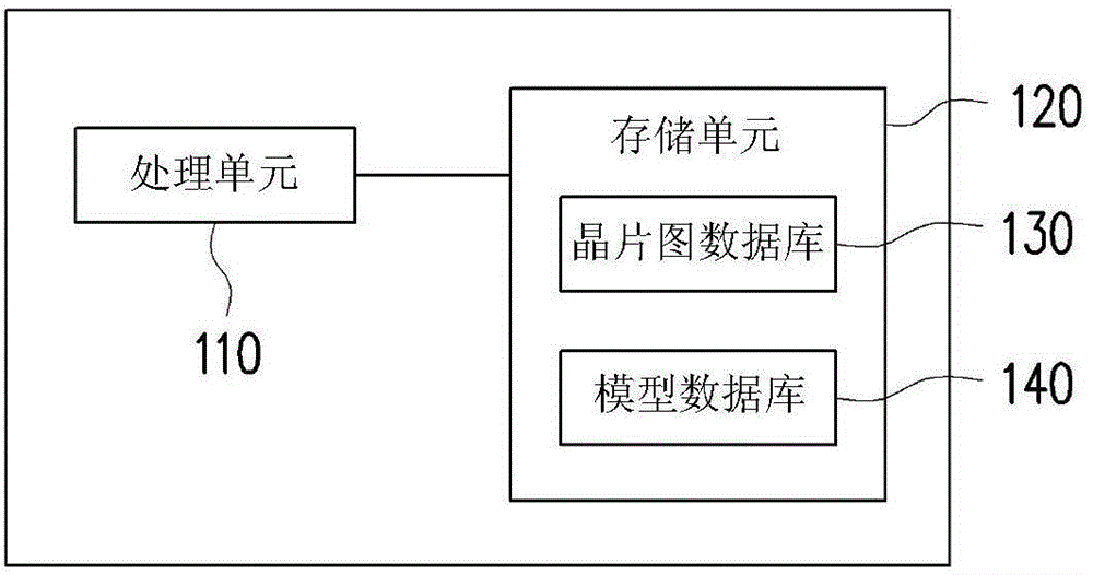
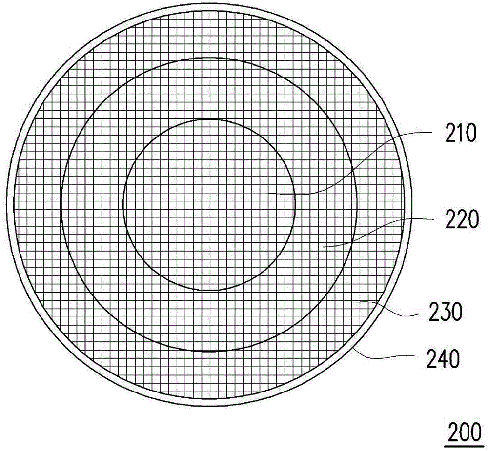
[0035] figure 1 is a block diagram of an electronic device according to an embodiment of the present invention. Please refer to figure 1 , the electronic device 100 includes a processing unit 110 and a storage unit 120 . The storage unit 120 includes a wafer map database 130 and a model database 140 . Here, the processing un...


PUM


Abstract

The invention provides a wafer test pattern yield loss calculation method comprising the following steps: grouping chips included in all test result categories in a wafer bin map to get multiple chip groups; getting multiple characteristic values of each chip group based on the chips included in each chip group; comparing the characteristic values with a model database to get test patterns corresponding to the chip groups; and calculating the yield loss of each test pattern. Therefore, a variety of test patterns in a wafer bin map can be identified automatically, and the yield loss of each test pattern can be calculated automatically.

Description

technical field [0001] The invention relates to a test mechanism of a wafer test pattern, in particular to a method for calculating the loss rate of the wafer test pattern. Background technique [0002] In the semiconductor manufacturing process, a wafer acceptance test (wafer acceptance test, WAT for short) is usually used to perform electrical testing on the wafer. WAT will generate a lot of electrical parameters and values, users can use these electrical parameters and values ​​to evaluate the yield of the wafer under test and discover possible problems in the semiconductor manufacturing process. However, in the semiconductor manufacturing process, when the wafer under test has a low yield rate, sometimes it is not caused by a single accident. In practice, different accident causes will result in different test patterns in the wafer bin map. Therefore, tracking the abnormal condition through the loss rate (Yield Loss) of the test pattern can usually have a good effect. ...

Claims


Application Information

Patent Timeline
IPC IPC(8): H01L21/66
Inventor 颜怀先
Owner WINBOND ELECTRONICS CORP
Why Eureka
Try Eureka