Semiconductor device
A semiconductor and housing technology, applied in the direction of semiconductor devices, semiconductor/solid-state device components, electric solid-state devices, etc., can solve the problems of high cost and increased manufacturing cost, and achieve the effect of suppressing increase and suppressing welding parts.
- Summary
- Abstract
- Description
- Claims
- Application Information
AI Technical Summary
Problems solved by technology
Method used
Image

Examples
no. 1 Embodiment approach
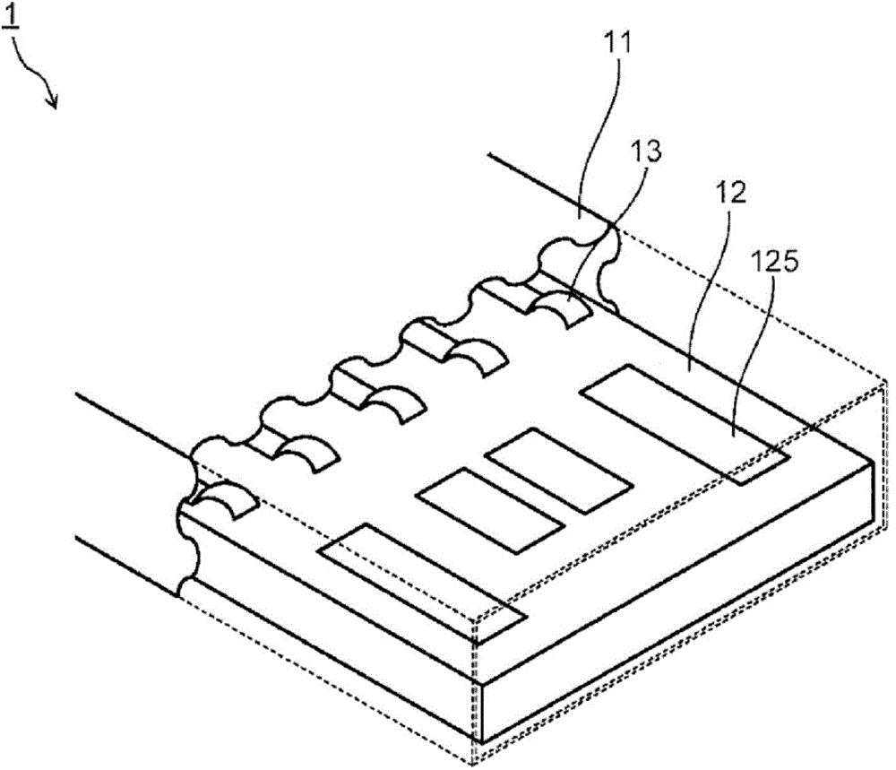
[0026] figure 1 It is a diagram showing a configuration example of a plug-integrated semiconductor device capable of data transfer using USB 3.0 by connecting to a socket. In addition, if it is a standard using the same signal, it can also be used as a semiconductor device that can perform data transfer using other USB standards. figure 1 The illustrated semiconductor device 1 includes a case 11 , a circuit board 12 having four external connection terminals 125 , and five external connection terminals 13 provided in the case 11 . figure 1 In , for the sake of convenience, a part of the housing 11 is indicated by a dotted line, and the boundary between the solid line and the dotted line is indicated by a wavy line.
[0027] As the external connection terminal 125, a power supply terminal (VBUS), a signal terminal (D+, D-) for normal transmission of a data signal as a differential signal, and a ground terminal (GND), etc. are provided using USB2.0 or USB3.0 An external connect...
no. 2 Embodiment approach
[0058] Figure 8 and Figure 9 It is a diagram showing a configuration example of a plug-type semiconductor device capable of performing data transfer by USB by connecting to a socket. Figure 8 is a schematic diagram viewed from the side direction, Figure 9 is a schematic view viewed from the upper surface direction. in addition, Figure 8 and Figure 9 In the figure, some components are not shown for the sake of convenience.
[0059] Figure 8 and Figure 9 The illustrated semiconductor device 2 includes a case 21 , a circuit board 22 , and a plug 23 . In addition, as the description of the case 21 and the circuit substrate 22, the figure 2 A description of the housing 11 and circuit substrate 12 is shown.
[0060] The housing 21 has an opening 210 . The inner wall of the opening 210 has an insertion hole 24a and a groove 24b. Although the planar shape of the insertion hole 24a and the groove part 24b is rectangular, it is not limited to this. In addition, the ...
no. 3 Embodiment approach
[0072] Figure 12 It is a diagram showing a structural example of a semiconductor device capable of data transfer using USB3.0 by connecting to a socket. In addition, if it is a standard using the same signal, it can also be used as a semiconductor device that can perform data transfer using other USB standards. Figure 12 The illustrated semiconductor device 3 includes a case 31 , a circuit board 32 , and external connection terminals 33 . In addition, as a description of the case 31, the circuit board 32, and the external connection terminal 33, it is possible to refer to figure 2 Description of the case 11, the circuit substrate 12, and the external connection terminals 13 shown.
[0073] The housing 31 has an opening 310 . A convex portion 311 is provided on an inner wall of the opening portion 310 . The housing 31 is formed of, for example, a material that can be applied to the housing 11 . For example, the housing 31 having the opening 310 may be formed by bonding ...
PUM
 Abstract
Description
Claims
Application Information
 - R&D
- Intellectual Property
- Life Sciences
- Materials
- Tech Scout
- Unparalleled Data Quality
- Higher Quality Content
- 60% Fewer Hallucinations
Browse by: Latest US Patents, China's latest patents, Technical Efficacy Thesaurus, Application Domain, Technology Topic, Popular Technical Reports.
© 2025 PatSnap. All rights reserved.Legal|Privacy policy|Modern Slavery Act Transparency Statement|Sitemap|About US| Contact US: help@patsnap.com