Display panel and manufacturing method thereof

A technology for display panels and manufacturing methods, applied in semiconductor/solid-state device manufacturing, semiconductor devices, electrical components, etc., can solve problems such as unfavorable aperture ratio, improvement, graphics density and machine capacity limitations, and increase the number of , Simplify the process, save the effect of the production process

Active Publication Date: 2016-10-12
WUHAN TIANMA MICRO ELECTRONICS CO LTD +1
View PDF7 Cites 11 Cited by
  • Summary
  • Abstract
  • Description
  • Claims
  • Application Information

AI Technical Summary

Problems solved by technology

On a display panel with a certain size, due to the limitation of the light-emitting area of ​​the reflective layer and the evaporation mask plate, it is not conducive to the improvement of the aperture ratio
Although the method of increasing the aperture ratio by reducing the aperture of the mask plate is a common method to improve the resolution of the device, it is limited by the pattern density and machine capability.

Method used


Image

  • Display panel and manufacturing method thereof
  • Display panel and manufacturing method thereof
  • Display panel and manufacturing method thereof

Examples


Embodiment Construction

[0059] The following will clearly and completely describe the technical solutions in the embodiments of the present invention with reference to the accompanying drawings in the embodiments of the present invention. Obviously, the described embodiments are only some, not all, embodiments of the present invention. Based on the embodiments of the present invention, all other embodiments obtained by persons of ordinary skill in the art without making creative efforts belong to the protection scope of the present invention.

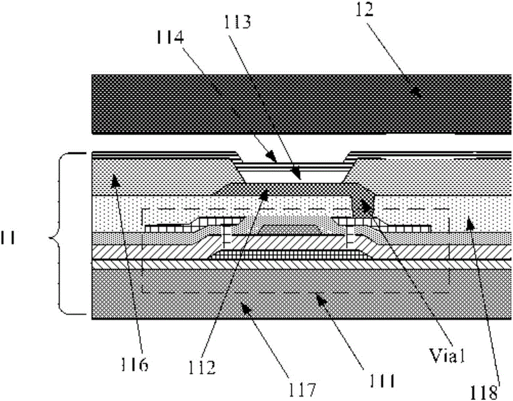
[0060] Such as figure 1 As shown, in the existing OLED display panel, on a display panel with a certain size, due to the limitation of the light-emitting area of ​​the reflective layer and the aperture of the evaporation mask, it is not conducive to the improvement of the aperture ratio. Although the method of increasing the aperture ratio by reducing the aperture of the mask plate is a common method to improve the resolution of the device, it is limited by th...


PUM


Abstract

The invention discloses a display panel and a manufacturing method. The display panel comprises a substrate, a planarizing layer and display units, wherein the planarizing layer is arranged on the surface of the substrate; the surface of the planarizing layer has adjusting structures; the planarizing layer comprises first regions and second regions; the surface of the first region is parallel to the substrate; the adjusting structure is located on the second region; the first regions and the second regions are alternately arranged at intervals; the display units cover the surfaces of the adjusting structures; and the adjusting structure is set to be a bump structure or a groove structure arranged in the second region. The adjusting structure is beneficial to an increase of the surface area of a light-emitting functional layer; the projection area of the light-emitting functional layer in the direction of the substrate is reduced; and the number of the display units is increased, so that the effect of improving the aperture ratio and the resolution ratio is achieved.

Description

technical field [0001] The present invention relates to the field of display technology, and more specifically, to a display panel and a manufacturing method thereof. Background technique [0002] With the continuous development of science and technology, more and more electronic devices with display functions are widely used in people's daily life and work, which brings great convenience to people's daily life and work. essential tool. A main component of an electronic device to realize a display function is a display panel, and an OLED display panel is one of the current mainstream display panels. [0003] refer to figure 1 , figure 1 It is a schematic structural diagram of a common OLED display panel in the prior art, and the OLED display panel includes: a cover plate 12 and an array substrate 11 that are oppositely arranged. The array substrate 11 includes: a substrate 117 , a TFT device 111 , a pixel definition layer 116 and a display unit. The TFT device 111 is lo...

Claims


Application Information

Patent Timeline
Patent Type & Authority Applications(China)
IPC IPC(8): H01L27/12H01L21/77
CPCH10K59/12
Inventor 刘海刘刚蒋卡恩尹招弟
Owner WUHAN TIANMA MICRO ELECTRONICS CO LTD
Why Eureka
Try Eureka