

Release film for printed circuit board production, method for producing release film for printed circuit board production, method for producing printed circuit board, and printed circuit board
A technology for a printed circuit substrate and a manufacturing method, which is applied in the field of release films for the manufacture of printed circuit substrates, can solve the problems of unevenness, local thickness of pinholes easily generated in the printed circuit substrate, etc. The effect of preventing breakage
- Summary
- Abstract
- Description
- Claims
- Application Information
AI Technical Summary
Problems solved by technology
Method used
Image

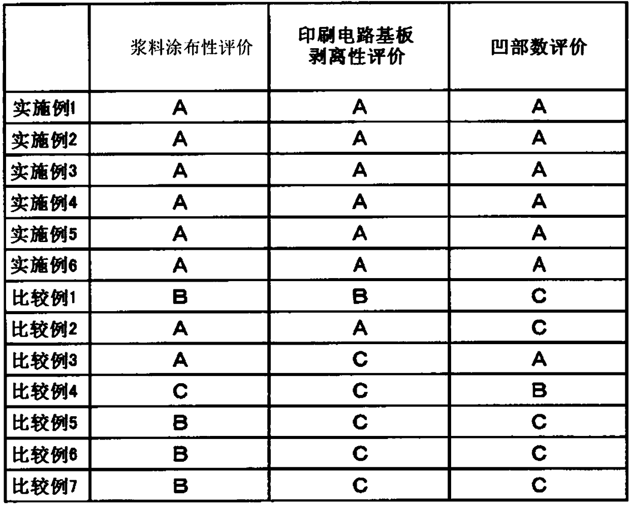
Examples
Embodiment 1
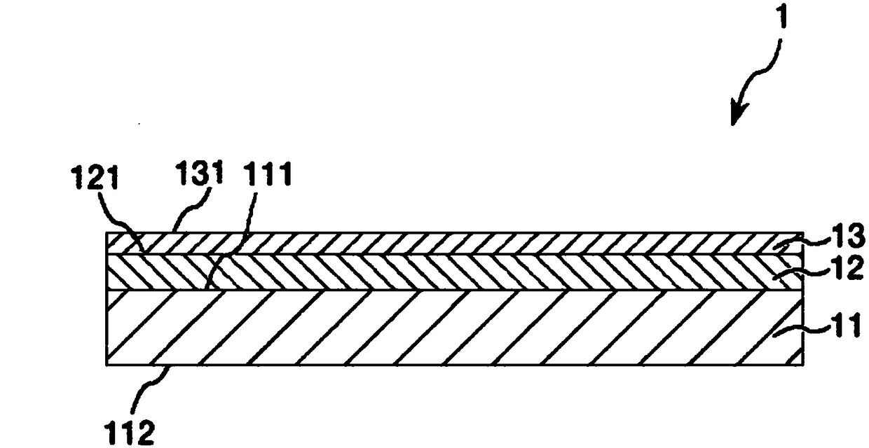
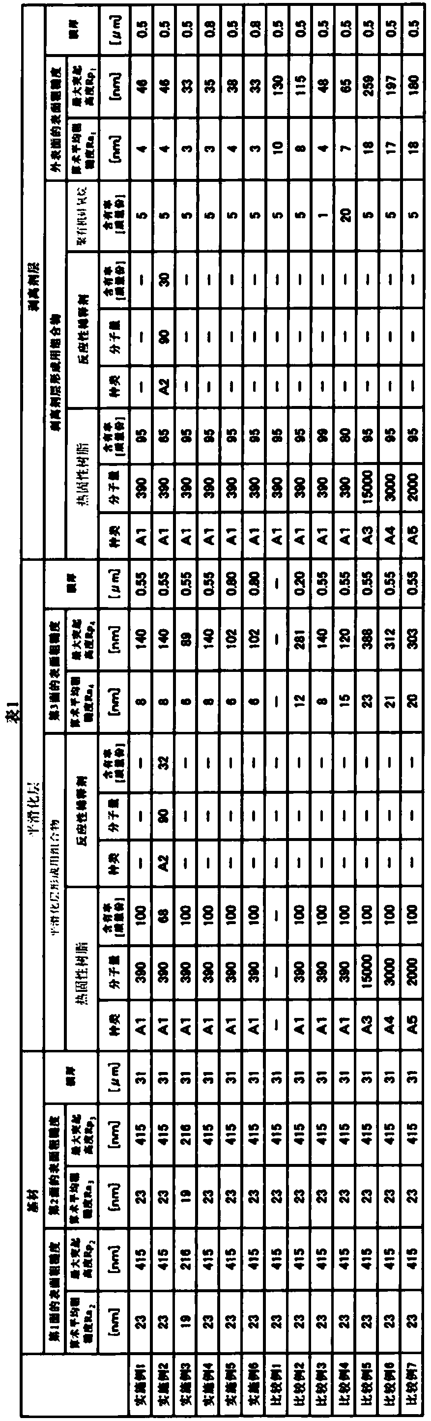
[0219] First, prepare a biaxially oriented polyethylene terephthalate film [thickness: 31 mm, arithmetic average roughness Ra of the first surface] as a base material 2 : 23nm, the maximum protrusion height Rp of the first surface 2 : 415nm, the arithmetic mean roughness Ra of the second surface 3 : 23nm, the maximum protrusion height Rp of the second surface 3 : 415nm].
[0220] Then, 100 parts by mass of melamine resin [manufactured by Mitsui Cytec Co., Ltd., trade name "Symel 303", hexamethoxymethylmelamine, mass average molecular weight 390, solid content 100 mass %], and 5 p-toluenesulfonic acid as an acidic catalyst Parts by mass and a mixed solvent (mass ratio 4 / 1) of isopropanol and isobutanol were mixed to obtain a composition for forming a smoothing layer with a solid content of 15% by mass.
[0221] Then, the obtained composition for smoothing layer formation was apply|coated on the 1st surface 111 of the base material 11 with the bar coater, and the 1st coating ...
Embodiment 2
[0225] Except having used the composition for smoothing layer formation obtained as follows, and the composition for release agent layer formation, it carried out similarly to Example 1, and manufactured the release film for printed circuit board manufacture.
[0226] Melamine resin [manufactured by Mitsui Cytec Corporation, trade name "Symer 303", hexamethoxymethylmelamine, mass average molecular weight 390, solid content 100% by mass] 65 parts by mass, and a diol compound [2- Methyl-1,3-propanediol, manufactured by Tokyo Chemical Industry Co., Ltd., mass average molecular weight 90, solid content 100%] In a mixture of 30 parts by mass, 5 parts by mass of p-toluenesulfonic acid as an acidic catalyst, and isopropanol and isopropanol A mixed solvent of butanol (mass ratio 4 / 1) was used to obtain a composition for forming a smoothing layer with a solid content of 15% by mass.
[0227] In addition, 65 parts by mass of melamine resin [manufactured by Mitsui Cytec Co., Ltd., trade ...
Embodiment 3
[0229] Except using biaxially oriented polyethylene terephthalate film [thickness: 31mm, arithmetic mean roughness Ra of the 1st side 2 : 19nm, the maximum protrusion height Rp of the first surface 2 : 216nm, the arithmetic mean roughness Ra of the second surface 3 : 19nm, the maximum protrusion height Rp of the second surface 3 : 216 nm], except that it was used as a base material, it carried out similarly to Example 1, and produced the release film for printed circuit board manufacture.
PUM
| Property | Measurement | Unit |
|---|---|---|
| thickness | aaaaa | aaaaa |
| surface roughness | aaaaa | aaaaa |
| particle size | aaaaa | aaaaa |
Abstract
Description
Claims
Application Information