Ultrawide-angle hemispherical lens antireflection film and coating method thereof
A technology of hemispherical lens and anti-reflection coating, which is applied in the field of ultra-wide-angle hemispherical lens anti-reflection coating and its coating. Risk of cracking, reduced reflectivity, uniform film thickness
- Summary
- Abstract
- Description
- Claims
- Application Information
AI Technical Summary
Problems solved by technology
Method used
Image
Examples
specific Embodiment
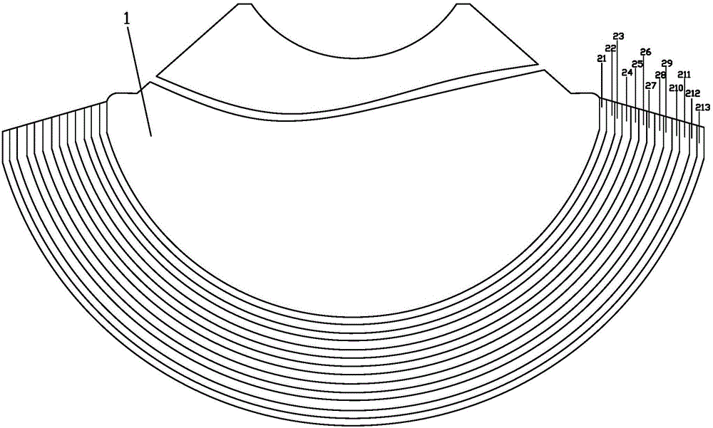
[0044] An anti-reflection coating for an ultra-wide-angle hemispherical lens. The anti-reflection coating 2 is composed of 13 layers plated on the lens body 1, wherein the 13 layers are as follows in the order from near to far away from the lens body: First SiO 2 Film layer 21, first TiO 2 Film layer 22, second SiO 2 Film layer 23, second TiO 2 Film layer 24, third SiO 2 Film layer 25, third TiO 2 Film layer 26, fourth SiO 2 Film layer 27, fourth TiO 2 Film layer 28, fifth SiO 2 Film layer 29, fifth TiO 2 Film layer 210, sixth SiO 2 Film 211, sixth TiO 2 Film 212 and MgF 2 膜层213。 Film layer 213.
[0045] The 13-layer film of the present invention is the minimum number of layers to achieve the effect of the present invention, but the thickness is not easy to control when the number of layers is larger, and it is not convenient for mass production.
[0046] The first SiO 2 The thickness of the film 21 is 20.0-22.0nm; the first TiO 2 The thickness of the film layer 22 is 11.1-13.1 nm; ...
Embodiment 1
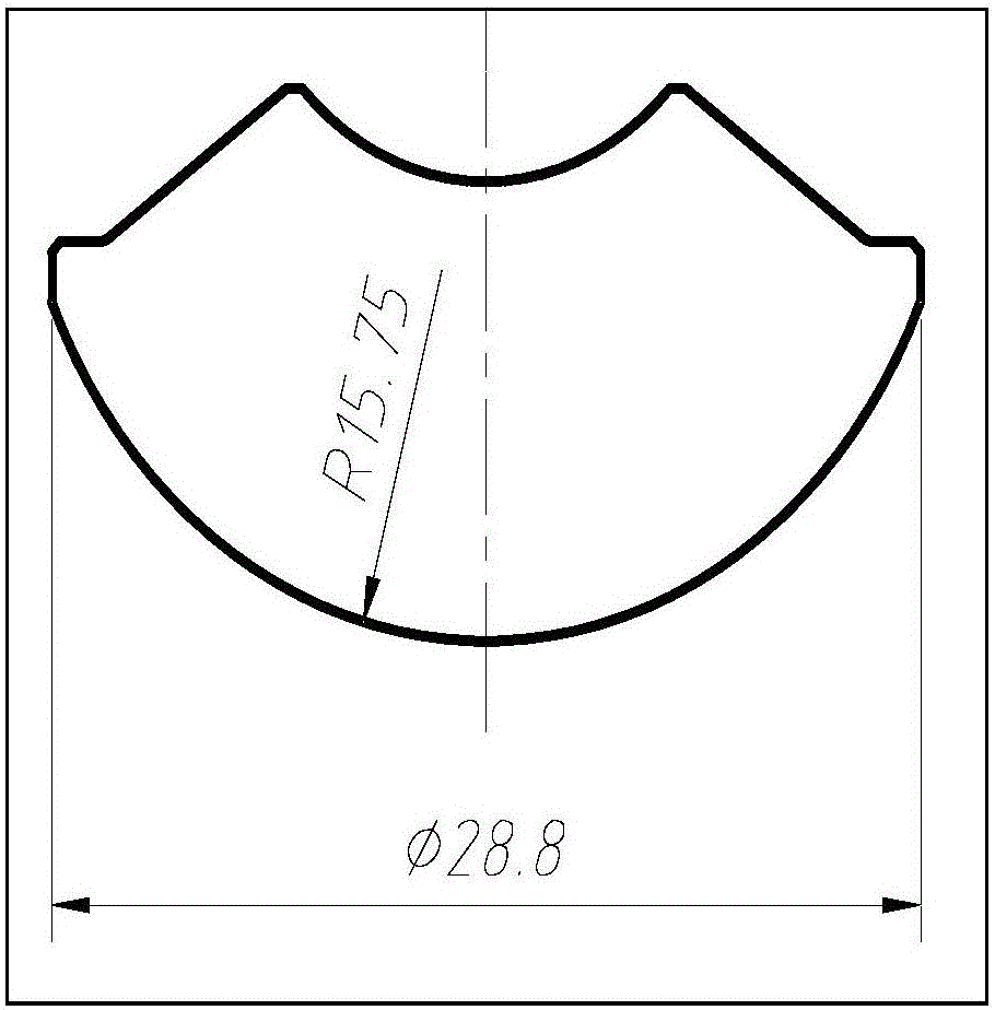
[0062] Such as figure 1 , The convex curvature of the ultra-wide-angle hemispherical lens is 15.75mm, the aperture is 28.8mm, and the spectral index requirements: Rabs <0.5%@420-700, the lens base material is ZF13.
[0063] A method for preparing the antireflection coating of an ultra-wide-angle hemispherical lens includes the following steps:
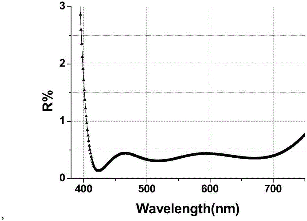
[0064] (1) Taking a conventional lens as an example, regardless of the film thickness difference between the edge and the center, a conventional visible light antireflection coating is pre-deposited to confirm the film thickness ratio between the center and the edge of the lens. Choose TiO 2 And SiO 2 The reflection spectrum designed as a coating material is such as image 3 As shown, the reflectivity of 420-700nm is less than 0.5%.
[0065] The film layers in order from near to far from the glass substrate are: the first layer, TiO with a thickness of 17.1nm 2 Film layer; the second layer, SiO with a thickness of 24.5nm 2 Film layer; the thi...
Embodiment 2
[0069] Choose TiO 2 , SiO 2 , MgF 2 As a coating material, the coating index confirmed in step 3 is R figure 2 As shown, the first layer, the first SiO with a thickness of 21nm 2 Film layer; the second layer, the first TiO with a thickness of 12.1nm 2 Film layer; the third layer, the second 53.5nm thick SiO 2 Film layer; the fourth layer, the second TiO with a thickness of 8.0nm 2 Film layer; the fifth layer, the third SiO with a thickness of 217.4nm 2 Film layer; the sixth layer, the third TiO with a thickness of 13.1nm 2 Film layer; the seventh layer, the fourth SiO with a thickness of 40.6nm 2 Film layer; the 8th layer, the fourth TiO with a thickness of 36nm 2 Film layer; the ninth layer, the fifth SiO with a thickness of 11.4nm 2 ; The 10th layer, the fifth TiO with a thickness of 78.6nm 2 Film layer; the 11th layer, the sixth SiO with a thickness of 23.2nm 2 Film layer; the 12th layer, the sixth SiO with a thickness of 23.9nm 2 Film layer: the 13th layer, a MgF2 film layer w...
PUM
| Property | Measurement | Unit |
|---|---|---|
| thickness | aaaaa | aaaaa |
| thickness | aaaaa | aaaaa |
| thickness | aaaaa | aaaaa |
Abstract
Description
Claims
Application Information


