Etching apparatus
An etching device and etching technology, which are used in the manufacture of electrical components, printed circuits, and the removal of conductive materials by chemical/electrolytic methods, can solve problems such as reducing product production efficiency, and achieve the effect of improving efficiency, ensuring suction, and reliable support.
- Summary
- Abstract
- Description
- Claims
- Application Information
AI Technical Summary
Problems solved by technology
Method used
Image

Examples
Embodiment Construction
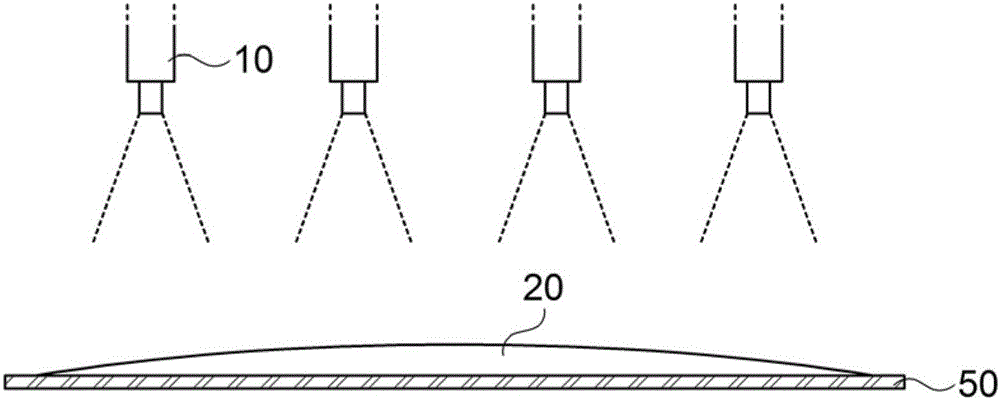
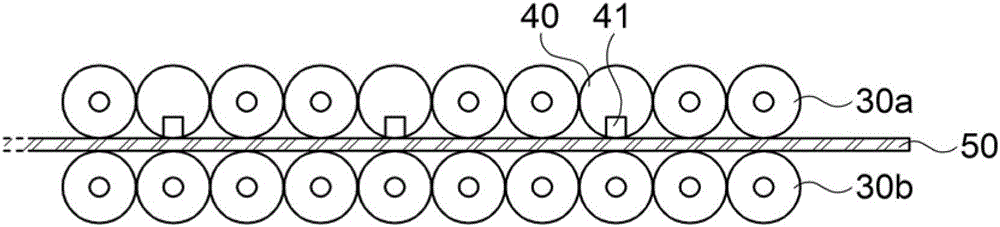
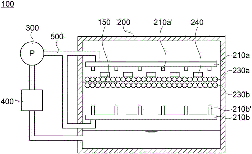
[0057] Below, refer to Figure 3 to Figure 11A specific example of an etching device according to an embodiment of the present invention will be described. However, this is only an exemplary embodiment, and the present invention is not limited thereto.
[0058] In the process of describing the embodiments of the present invention, if it is considered that the specific description of the known technology related to the present invention may cause unnecessary confusion to the gist of the present invention, its detailed description will be omitted. In addition, the terms described below are all terms defined in consideration of the functions in the present invention, and may vary depending on the user's or operator's intention or custom. Therefore, it needs to be defined based on the contents throughout the specification.
[0059] The technical idea of the present invention is determined by the scope of the claims, and the following examples are only a means to effectively ex...
PUM
 Abstract
Description
Claims
Application Information
 - R&D
- Intellectual Property
- Life Sciences
- Materials
- Tech Scout
- Unparalleled Data Quality
- Higher Quality Content
- 60% Fewer Hallucinations
Browse by: Latest US Patents, China's latest patents, Technical Efficacy Thesaurus, Application Domain, Technology Topic, Popular Technical Reports.
© 2025 PatSnap. All rights reserved.Legal|Privacy policy|Modern Slavery Act Transparency Statement|Sitemap|About US| Contact US: help@patsnap.com