a snubber circuit

A buffer circuit and pulse circuit technology, which is applied in the direction of logic circuit, logic circuit connection/interface layout, pulse technology, etc., can solve the problems of slow loop response speed and small bandwidth of traditional buffer circuits, and improve the loop response speed , the effect of large bandwidth

Active Publication Date: 2019-06-11
HEFEI GEYI INTEGRATED CIRCUIT CO LTD +1
View PDF5 Cites 0 Cited by
  • Summary
  • Abstract
  • Description
  • Claims
  • Application Information

AI Technical Summary

Problems solved by technology

[0004] However, since the capacitor C3 in the buffer circuit of the above-mentioned traditional buffer connects the P-type field effect transistor P7 to the output signal terminal V out , resulting in the main pole w1=1 / (Rs×gm7×R4×C3) in the traditional snubber circuit, wherein the above w1 represents the above-mentioned main pole, Rs represents the output resistance of the first-stage circuit, and gm7 represents the P-type field effect transistor The transconductance of P7, due to the existence of gm7 in the traditional buffer circuit, and the above-mentioned gm7×R4 is far greater than 1, so the above-mentioned capacitor C3 is amplified, resulting in a smaller dominant pole, because the dominant pole represents the maximum value of the signal frequency , the dominant pole is small, indicating that the available frequency range is small, and then it can be seen that the bandwidth of the traditional snubber circuit is small, which makes the loop response speed of the traditional snubber circuit slower

Method used


Image

  • a snubber circuit
  • a snubber circuit
  • a snubber circuit

Examples


Embodiment 1

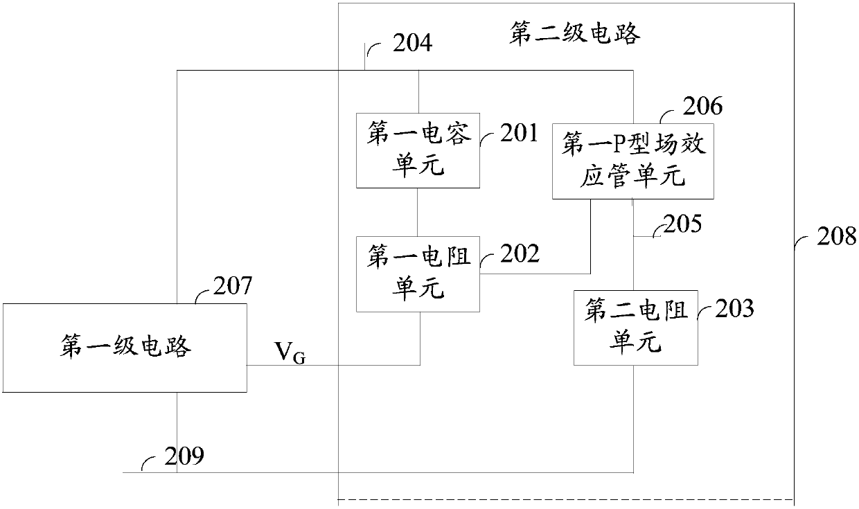
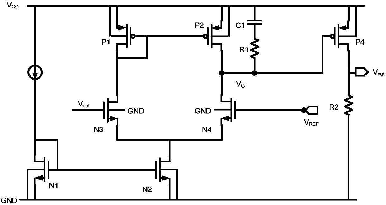
[0027] refer to figure 2 , shows a schematic structural diagram of Embodiment 1 of a buffer circuit of the present invention, the buffer circuit may specifically include a first-stage circuit 207 and a second-stage circuit 208; wherein, the second-stage circuit 208 may specifically include: A capacitance unit 201, a first resistance unit 202, a second resistance unit 203, an input terminal 204, an output signal terminal 205, and a first P-type field effect transistor unit 206; wherein, one end of the first capacitance unit 201 is connected to the Input terminal 204, the other end is connected to one end of the first resistance unit 202; the other end of the first resistance unit 202 is respectively connected to the output terminal V of the first stage circuit G , the gate of the first P-type field effect transistor unit 206; the source of the first P-type field effect transistor unit 206 is connected to the input terminal 204, and the drain is connected to the output signal t...

Embodiment 2

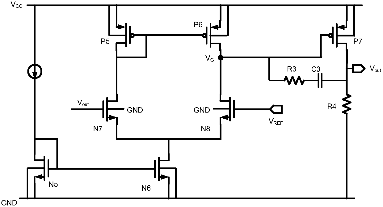
[0036] refer to Figure 4 , shows a schematic structural diagram of a buffer circuit embodiment 2 of the present invention, the buffer circuit may specifically include a first-stage circuit and a second-stage circuit; wherein, the second-stage circuit includes: a first capacitor unit 401 , the first resistance unit 402, the second resistance unit 403, the input terminal 404, the output signal terminal 405, the first P-type field effect tube unit 406, the pulse circuit unit 407, the second P-type field effect tube unit 408, and the second capacitance Unit 409, an input signal terminal 410; wherein, one end of the first capacitor unit 401 is connected to the input terminal 404, and the other end is connected to one end of the first resistance unit 402; the other ends of the first resistance unit 402 are respectively Connect the output terminal VG of the first stage circuit and the first P-type field effect transistor unit 406; the first P-type field effect transistor unit 406 is...


PUM


Abstract

An embodiment of the present invention provides a buffer circuit. The buffer circuit includes a first-stage circuit and a second-stage circuit; wherein, the second-stage circuit includes: a first capacitor unit, a first resistor unit, and a second resistor A unit, an input terminal, an output signal terminal, and a first P-type field effect transistor unit; wherein, one end of the first capacitance unit is connected to the input end, and the other end is connected to one end of the first resistance unit; the first The other end of the resistance unit is respectively connected to the output terminal of the first stage circuit and the gate of the first P-type field effect transistor unit; the source of the first P-type field effect transistor unit is connected to the input terminal, The drain is connected to the output signal end; one end of the second resistance unit is connected to the output signal end, and the other end is grounded. The embodiments of the present invention can bring greater bandwidth, thereby improving the loop response speed of the buffer circuit.

Description

technical field [0001] The invention relates to the field of circuits, in particular to a buffer circuit. Background technique [0002] With the rapid growth of the electronic product market, the buffers used in these electronic products have also developed rapidly. [0003] refer to figure 1 , which shows a structural schematic diagram of an existing traditional buffer buffer circuit, the circuit is a two-stage circuit, wherein the above circuit specifically includes: 4 N-type field effect transistors (N5, N6, N7, N8), 3 P-type field effect transistors (P5, P6, P7), 2 resistors (R3, R4), 1 capacitor C3, input signal terminal V REF , and the output signal terminal V out ; Wherein, the drain of the above-mentioned N5 is connected to the power supply terminal VCC, the gate of N5 is connected to the gate of the above-mentioned N6 and the power supply terminal VCC respectively, the drain of N6 is connected to the sources of N7 and N8 respectively, and the drain of N7 is conne...

Claims


Application Information

Patent Timeline
Patent Type & Authority Patents(China)
IPC IPC(8): H03K19/0185
CPCH03K19/018507
Inventor 方海彬刘铭
Owner HEFEI GEYI INTEGRATED CIRCUIT CO LTD
Why Eureka
Try Eureka