Embedded type semiconductor chip fan-out type packaging structure and manufacturing method therefor

A packaging structure and semiconductor technology, applied in semiconductor/solid-state device manufacturing, semiconductor devices, semiconductor/solid-state device components, etc., can solve the problems of increasing metal line stress, height difference, and difficulty in ensuring that the surface of the chip is consistent with the surface of the substrate, etc. To achieve the effect of ensuring flatness and expanding the application range

Inactive Publication Date: 2016-11-09
HUATIAN TECH KUNSHAN ELECTRONICS
View PDF5 Cites 14 Cited by
  • Summary
  • Abstract
  • Description
  • Claims
  • Application Information

AI Technical Summary

Problems solved by technology

However, when the chip is embedded in the silicon substrate, due to process or design reasons, the chip may be lower or higher than the substrate surface, and it is difficult to ensure that all chip surfaces are consistent with the substrate surface
If the height difference is large, it will lead to uneven metal lines on the upper insulating layer, increasing the stress on the metal lines, and there is a hidden danger that the metal lines will be broken
And when the solder balls are added later, there is a height difference between the solder balls on the chip and the solder balls fanned out to the substrate, and there will also be reliability problems when the chip is soldered to the external circuit board

Method used


Image

  • Embedded type semiconductor chip fan-out type packaging structure and manufacturing method therefor
  • Embedded type semiconductor chip fan-out type packaging structure and manufacturing method therefor
  • Embedded type semiconductor chip fan-out type packaging structure and manufacturing method therefor

Examples


Embodiment Construction

[0037] The following will clearly and completely describe the technical solutions in the embodiments of the present invention with reference to the accompanying drawings in the embodiments of the present invention. Obviously, the described embodiments are only some, not all, embodiments of the present invention. Based on the embodiments of the present invention, all other embodiments obtained by persons of ordinary skill in the art without making creative efforts belong to the protection scope of the present invention.

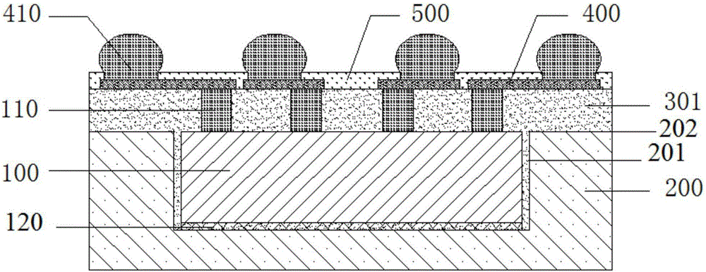
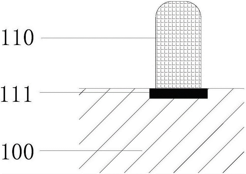
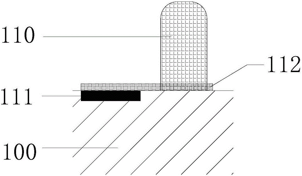
[0038] figure 1 A cross-sectional view of an embedded semiconductor chip fan-out package structure according to an embodiment of the present invention is shown. Such as figure 1 , figure 2 , image 3 As shown, the embedded semiconductor chip fan-out package structure includes at least one chip 100 (one is taken as an example in this embodiment) and a semiconductor substrate 200 . A plurality of conductive pads are disposed on the front of the chip 100 , e...


PUM


Abstract

The invention discloses an embedded semiconductor chip fan-out packaging structure and a manufacturing method thereof. The packaging structure includes a semiconductor substrate and a chip. A plurality of conductive pads are arranged on the front side of the chip, and the semiconductor substrate is provided with a receiving groove, and the chip is accommodated in the receiving groove with the front facing outward. A metal post is grown on each conductive pad, and the metal post is higher than the upper surface of the semiconductor substrate. The gap between the receiving groove and the chip, the upper surface and the surroundings of the metal post are filled or covered by an insulating layer. A metal rewiring is connected to the top surfaces of all the metal pillars, and at least one metal rewiring extends beyond the surface of the chip. In the present invention, metal pillars are long on the chip, and the chip and the metal pillars are covered with polymer materials, and then the metal pillars of the chip are exposed by using a planarization process, so as to ensure the flatness of the surface of the package; meanwhile, the size range of the groove can be expanded . The invention also discloses a manufacturing method of the embedded semiconductor chip fan-out packaging structure.

Description

technical field [0001] The invention relates to a chip fan-out packaging structure and a manufacturing method thereof in the technical field of semiconductor packaging, in particular to an embedded semiconductor chip fan-out packaging structure and a manufacturing method thereof. Background technique [0002] The company has always paid attention to the research of chip packaging technology, such as the "Buried Silicon Substrate Fan-Out Type package structure and manufacturing method thereof". However, when the chip is embedded in the silicon substrate, due to process or design reasons, the chip may be lower or higher than the substrate surface, and it is difficult to ensure that all chip surfaces are consistent with the substrate surface. If the height difference is large, the metal circuit on the upper insulating layer will be uneven, increasing the stress on the metal circuit, and there is a hidden danger that the metal circuit will be broken. And when the solder balls ...

Claims


Application Information

Patent Timeline
Patent Type & Authority Applications(China)
IPC IPC(8): H01L23/485H01L23/31H01L21/60H01L21/56
CPCH01L24/19H01L24/20H01L24/97H01L2224/04105H01L2224/12105H01L2224/32225H01L2224/73267H01L2224/92244H01L2224/97H01L2924/15153H01L2924/157H01L2924/18162H01L23/31H01L21/56H01L24/27H01L24/30H01L2224/301H01L2224/30104
Inventor 翟玲玲于大全
Owner HUATIAN TECH KUNSHAN ELECTRONICS
Why Eureka
Try Eureka