Infrared detection picture element structure, manufacturing method therefor and hybrid imaging device

A technology of pixel structure and infrared detection, which is applied in the direction of electrical components, electric radiation detectors, radiation pyrometry, etc., can solve the problems of low sensitivity of imaging devices, degradation of imaging quality, inconsistent correspondence of single imaging units, etc., to improve sensitivity , Improving the effect of image quality

Active Publication Date: 2016-11-16
SHANGHAI INTEGRATED CIRCUIT RES & DEV CENT
View PDF4 Cites 14 Cited by
  • Summary
  • Abstract
  • Description
  • Claims
  • Application Information

AI Technical Summary

Problems solved by technology

[0003] In the prior art, two imaging chips with different bands and two sets of optical paths are used to realize visible light imaging and long-wave band signal imaging respectively, and they are synthesized together through computer algorithm processing. Due to the inconsistency of optical paths and the corresponding error of a single imaging unit, there will be Causes a large deviation in the composite image, which seriously affects the imaging quality and monitoring effect; in addition, due to the low sensitivity of this imaging device, it further leads to a decline in imaging quality

Method used


Image

  • Infrared detection picture element structure, manufacturing method therefor and hybrid imaging device
  • Infrared detection picture element structure, manufacturing method therefor and hybrid imaging device
  • Infrared detection picture element structure, manufacturing method therefor and hybrid imaging device

Examples


Embodiment Construction

[0031] In order to make the content of the present invention clearer and easier to understand, the content of the present invention will be further described below in conjunction with the accompanying drawings. Of course, the present invention is not limited to this specific embodiment, and general replacements known to those skilled in the art are also covered within the protection scope of the present invention.

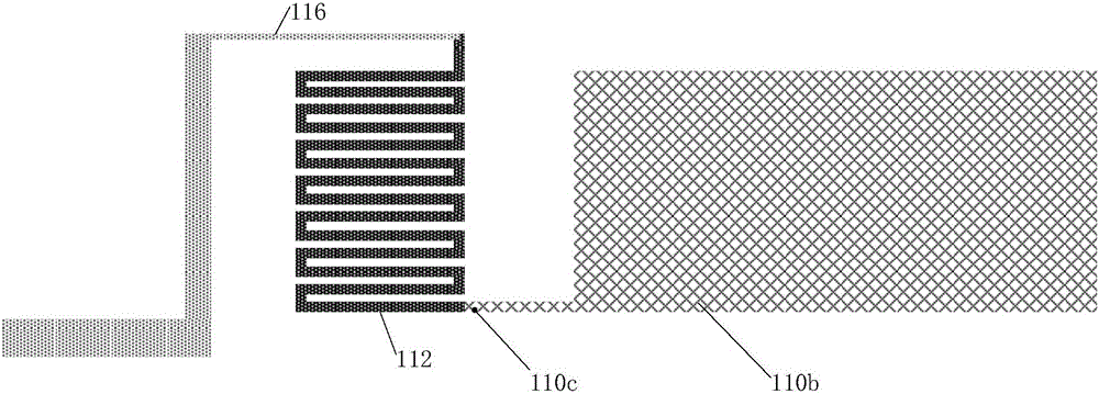
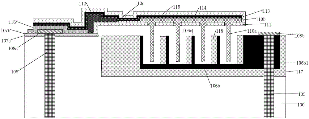
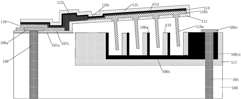
[0032] The infrared detection pixel structure of the present invention utilizes an upper electrode structure and a lower electrode structure with one end fixed and the other end not fixed, the upper electrode structure of the upper electrode structure and the lower electrode structure of the lower electrode structure are arranged alternately, on the upper electrode structure With an infrared sensitive structure, the infrared sensitive structure is used to absorb infrared light and produce thermal deformation to cause relative displacement of the upper electrode stru...


PUM


Abstract

The invention provides an infrared detection picture element structure, a manufacturing method therefor and a hybrid imaging device. Upper and lower pole plates having a comb structure can be used for forming a capacitor structure, and one end of an upper electrode structure cannot be fixed; when an infrared sensitive structure in the upper electrode structure absorbs infrared light so as to generate heat stress, deformation is caused, change of capacitance between the upper and lower pole plates is caused, infrared detection can be realized, device sensitivity can be improved, the infrared detection picture element structure can be applied to an infrared light and visible light hybrid imaging device, visible imaging and infrared imaging on the same silicon substrate can be realized, and imaging quality can be improved.

Description

technical field [0001] The invention relates to the technical field of semiconductors, in particular to an infrared detection pixel structure and a preparation method thereof, and a hybrid imaging device. Background technique [0002] With the wide application of imaging monitoring systems in daily life, monitoring systems that only use 300nm-900nm visible light band imaging are increasingly unable to meet the monitoring requirements of environments such as nighttime or high dynamic changes. Imaging of optical signals outside the band, especially long-wave bands (including signals in infrared, THZ and other bands); [0003] In the prior art, two imaging chips with different wavelength bands and two sets of optical paths are used to realize visible light imaging and long-wave band signal imaging respectively, and they are combined through computer algorithm processing. Due to the inconsistency of optical paths and the corresponding error of a single imaging unit, there will ...

Claims


Application Information

Patent Timeline
Patent Type & Authority Applications(China)
IPC IPC(8): G01J5/34
CPCG01J5/34G01J2005/0077H04N5/33G01J5/40G01J5/024H10N15/10
Inventor 康晓旭陈寿面
Owner SHANGHAI INTEGRATED CIRCUIT RES & DEV CENT
Why Eureka
Try Eureka