Thin film transistor array substrate and manufacturing method therefor

A thin-film transistor and manufacturing method technology, applied in the field of thin-film transistor array substrates and its manufacturing, can solve the problems of complicated production process and increased production cost, and achieve the effects of simplifying the processing process steps, reducing production cost, and saving patterning process

Active Publication Date: 2016-11-16
TCL CHINA STAR OPTOELECTRONICS TECH CO LTD
View PDF6 Cites 11 Cited by
  • Summary
  • Abstract
  • Description
  • Claims
  • Application Information

AI Technical Summary

Problems solved by technology

[0002] In the prior art (Fringe Field Switching abbreviated as FFS) mode thin film transistors have a large viewing angle and transmittance and are widely used at present. Usually, 6-8 times of mask (exposure) are usually required in the manufacturing process of thin film transistor array substrates. For the formation of gate lines and gates, active layer, etch barrier layer, source and drain, passivation layer, electrodes and vias, etc., the production process is complicated and the production cost increases accordingly

Method used


Image

  • Thin film transistor array substrate and manufacturing method therefor
  • Thin film transistor array substrate and manufacturing method therefor
  • Thin film transistor array substrate and manufacturing method therefor

Examples


Embodiment Construction

[0032] The following will clearly and completely describe the technical solutions in the embodiments of the present invention with reference to the accompanying drawings in the embodiments of the present invention. Obviously, the described embodiments are only some, not all, embodiments of the present invention. Based on the embodiments of the present invention, all other embodiments obtained by persons of ordinary skill in the art without making creative efforts belong to the protection scope of the present invention.

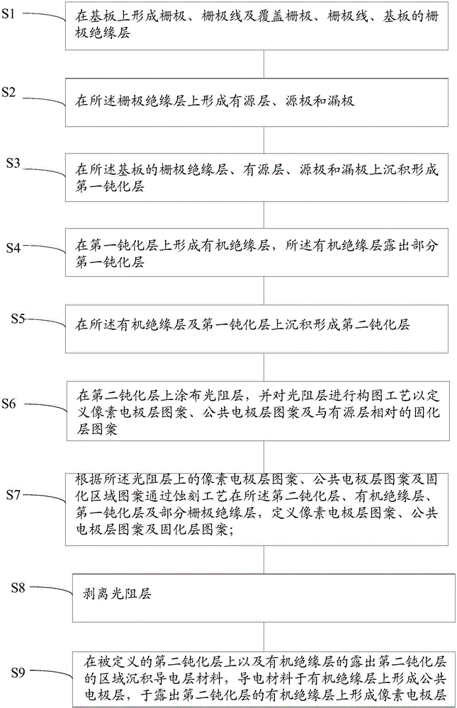
[0033] see figure 1 , which is a flowchart of a manufacturing method of a thin film transistor according to a preferred embodiment of the present invention. The manufacturing method of the thin film transistor (thin film transistor, TFT) includes the following steps.

[0034] Step S1: forming a gate, a gate line, and a gate insulating layer covering the gate, the gate line, and the substrate on the substrate.

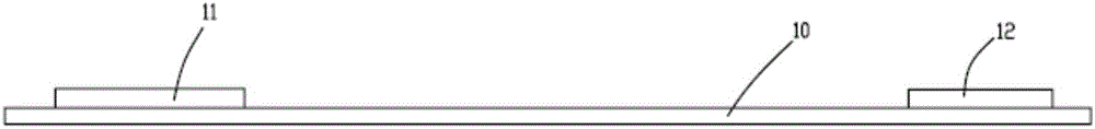
[0035] see figure 2 , specifically includes, ...


PUM


Abstract

The invention provides a manufacturing method for a thin film transistor. The manufacturing method comprises the steps of forming a first passivation layer, an organic insulating layer and a second passivation layer on a gate electrode insulating layer, an active layer, and a source electrode and a drain electrode of a substrate through deposition in sequence; coating the second passivation layer with a photoresist layer, performing a patterning process on the photoresist layer to define a pixel electrode layer pattern, a common electrode layer pattern and a pattern of a curing layer which is opposite to the active layer; defining the pixel electrode layer pattern, the common electrode layer pattern and the curing layer pattern through an etching process on the second passivation layer, the organic insulating layer, the first passivation layer and a part of the gate electrode insulating layer, and peeling off the photoresist layer; and forming a common electrode layer on the defined insulating layer, and forming the pixel electrode layer on the organic insulating layer where the second passivation layer is exposed.

Description

technical field [0001] The invention relates to the field of manufacturing thin film transistors, in particular to a thin film transistor array substrate and a manufacturing method thereof. Background technique [0002] In the prior art (Fringe Field Switching abbreviated as FFS) mode thin film transistors have a large viewing angle and transmittance and are widely used at present. Usually, 6-8 times of mask (exposure) are usually required in the manufacturing process of thin film transistor array substrates. For the formation of gate lines and gates, active layer, etch stop layer, source and drain, passivation layer, electrodes and vias, etc., the production process is complicated, and the production cost increases accordingly. Contents of the invention [0003] The invention provides a thin film transistor array substrate and a manufacturing method, which can reduce the number of exposures, simplify the manufacturing process, and reduce the cost. [0004] The manufactur...

Claims


Application Information

Patent Timeline
Patent Type & Authority Applications(China)
IPC IPC(8): H01L27/12
CPCH01L27/1288H01L21/02271H01L21/0274H01L21/47573H01L27/12H01L27/1225H01L27/124H01L27/1248H01L27/1262H01L29/4908H01L29/66969H01L29/7869H01L27/1214H01L27/1259
Inventor 卢马才
Owner TCL CHINA STAR OPTOELECTRONICS TECH CO LTD
Why Eureka
Try Eureka