
Touch panel and bonding structure thereof

A bonding structure and touch panel technology, which is applied in the direction of instruments, electrical digital data processing, and data processing input/output process, etc., can solve the problems of large differences in tension values, insufficient bonding strength between bonding pads and circuit boards, and insufficient tension values. Uniformity and other issues, to achieve the effect of improving the binding force, not easy to separate, and uniform tension value

Inactive Publication Date: 2016-11-23
TPK TOUCH SYST XIAMEN
View PDF3 Cites 11 Cited by
  • Summary
  • Abstract
  • Description
  • Claims
  • Application Information

AI Technical Summary

Problems solved by technology

If the circuit board cannot be firmly attached to the bonding pad, the touch panel will not work properly
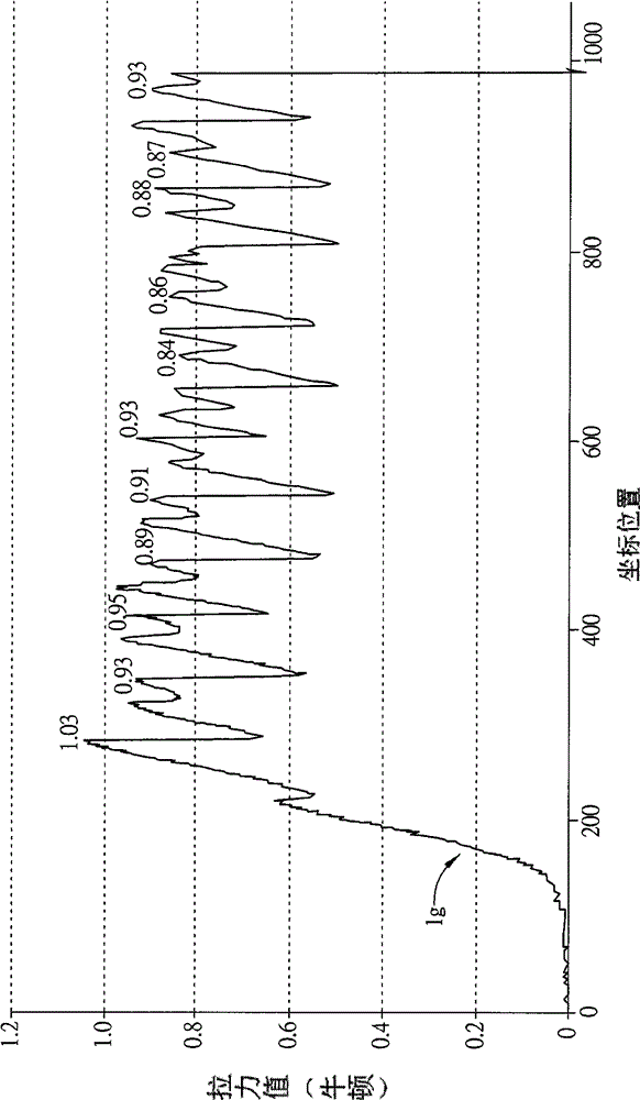
The conventional bonding pads are long strips with a single width and are arranged at intervals in sequence. The gaps between the bonding pads and the adjacent bonding pads produce a large difference in tensile force value, and the tensile value is uneven, resulting in the bonding strength between the bonding pad and the circuit board. not enough

Method used


Image

  • Touch panel and bonding structure thereof
  • Touch panel and bonding structure thereof
  • Touch panel and bonding structure thereof

Examples


Embodiment Construction

[0056] The present invention will be further described in detail below in conjunction with the accompanying drawings and specific embodiments.

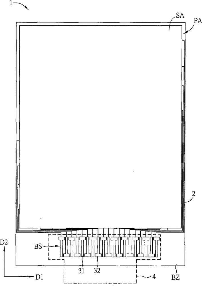
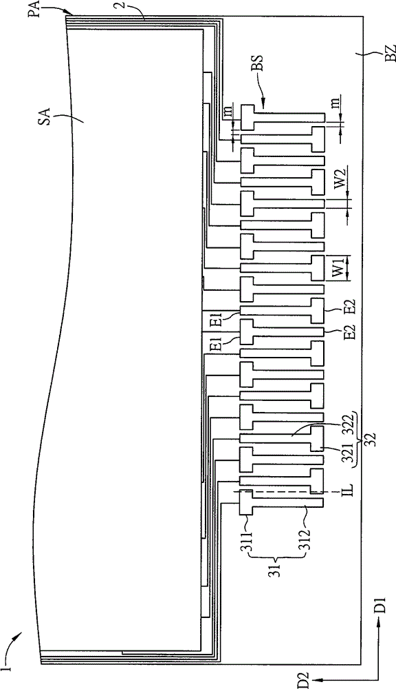
[0057] Figure 1A It is a schematic diagram of a touch panel 1 according to the first embodiment of the present invention, Figure 1B for Figure 1A A partially enlarged schematic diagram of the touch panel 1 shown. Please also refer to Figure 1A and Figure 1BAs shown, the touch panel 1 includes a sensing area SA, a peripheral area PA, a bonding structure BS, and a plurality of wires 2 . The touch panel 1 can use resistive, capacitive, optical or other touch technologies, wherein the sensing area SA can undergo corresponding structural changes according to the above touch technologies, and no limitation is imposed here. In addition, the "touch panel" referred to herein may include a touch panel or a touch display panel, and the "junction structure" may be applicable not only to a touch panel, but also to other electronic devices s...


PUM


Abstract

The invention provides a touch panel and a bonding structure thereof. The bonding structure comprises multiple first bonding pads and multiple second bonding pads. The first bonding pads are arranged in a bonding area in sequence in the first direction, and the second bonding pads and the first bonding pads are alternately arranged in the bonding area in sequence in the first direction; the second bonding pads and the first bonding pads are electrically insulated from each other, and projection locations of the adjacent first bonding pads and second bonding pads in the first direction are partially overlapped or tangent. Therefore, the bonding strength of the bonding pads and a circuit board can be improved.

Description

technical field [0001] The invention relates to a touch panel and its bonding structure. Background technique [0002] With the rapid development of science and technology, touch technology has become common in daily life, such as cash machines, electronic ticket vending machines, information inquiry systems or access control identification systems, etc., and even portable electronic devices such as smart phones, tablet computers or notebook computers . [0003] In the current common touch technology, the signal of the touch sensing area is transmitted to the circuit board through the wire, and then the signal is transmitted to the controller through the circuit board, so that the controller can perform subsequent processing of the touch signal. The circuit board is usually electrically connected to the wires through bonding pads attached to the touch panel. If the circuit board cannot be firmly attached to the bonding pads, the touch panel will not function properly. The...

Claims


Application Information

Patent Timeline
Patent Type & Authority Applications(China)
IPC IPC(8): G06F3/041
Inventor 洪浦地李瑞兴张普欣吴荣林陈福城
Owner TPK TOUCH SYST XIAMEN
Learn More