Quantum dot film, its manufacturing method and display device
A production method and technology of quantum dot film, applied in the optical field, can solve the problems of high cost and complicated pixel isolation structure process, and achieve the effect of reducing production cost and solving color accuracy.
- Summary
- Abstract
- Description
- Claims
- Application Information
AI Technical Summary
Problems solved by technology
Method used
Image

Examples
Embodiment 1
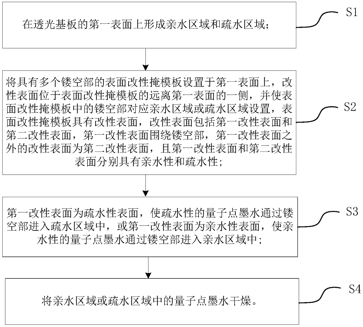
[0045] The steps of the method for fabricating a surface-modified mask provided in this embodiment include:
[0046] Step S01, immersing the mask in a solution with a hydrophobic material, the hydrophobic material being heptadecafluorodecyltrimethoxysilane, so that the hydrophobic material is fixed on the surface of the mask;
[0047] Step S02, separating the mask plate immobilized with the hydrophobic material from the solution, and drying the mask plate;
[0048] Step S03, placing the first mask on the first surface of the mask plate with 96×64 hollowed-out parts, the first mask is composed of 96×64 first shielding parts and first transparent parts connecting each first shielding part. Composition of light parts, the first shielding part corresponds to the hollow part one by one, and the area of each first shielding part in one-to-one correspondence is larger than the area of each hollow part, and the UV lamp is used to emit ultraviolet light with a wavelength of 185nm a...
Embodiment 2
[0050] The manufacturing method of the surface-modified light-transmitting substrate provided in this embodiment is as follows:
[0051] Mix the coupling agent and initiator in a solvent to form a substrate treatment solution, place one side of the transparent substrate in the substrate treatment solution, and bond and fix the coupling agent on the surface of the transparent substrate to form a bond surface, the first reaction raw material is arranged on the bonding surface, the first reaction raw material located in the first area is covered, and the first reaction raw material located in the second area is irradiated with ultraviolet rays, so that the first reaction raw material and the coupling agent The grafting reaction is carried out under ultraviolet irradiation, thereby forming a hydrophobic region, removing the first reaction raw material in the first region, setting the second reaction raw material on the first region and the second covering region, and covering the s...
Embodiment 3
[0054] The manufacturing method of the quantum dot film provided in this embodiment adopts the surface-modified mask plate in Embodiment 1 and the surface-modified light-transmitting substrate in Embodiment 2, and the manufacturing method includes the following steps:
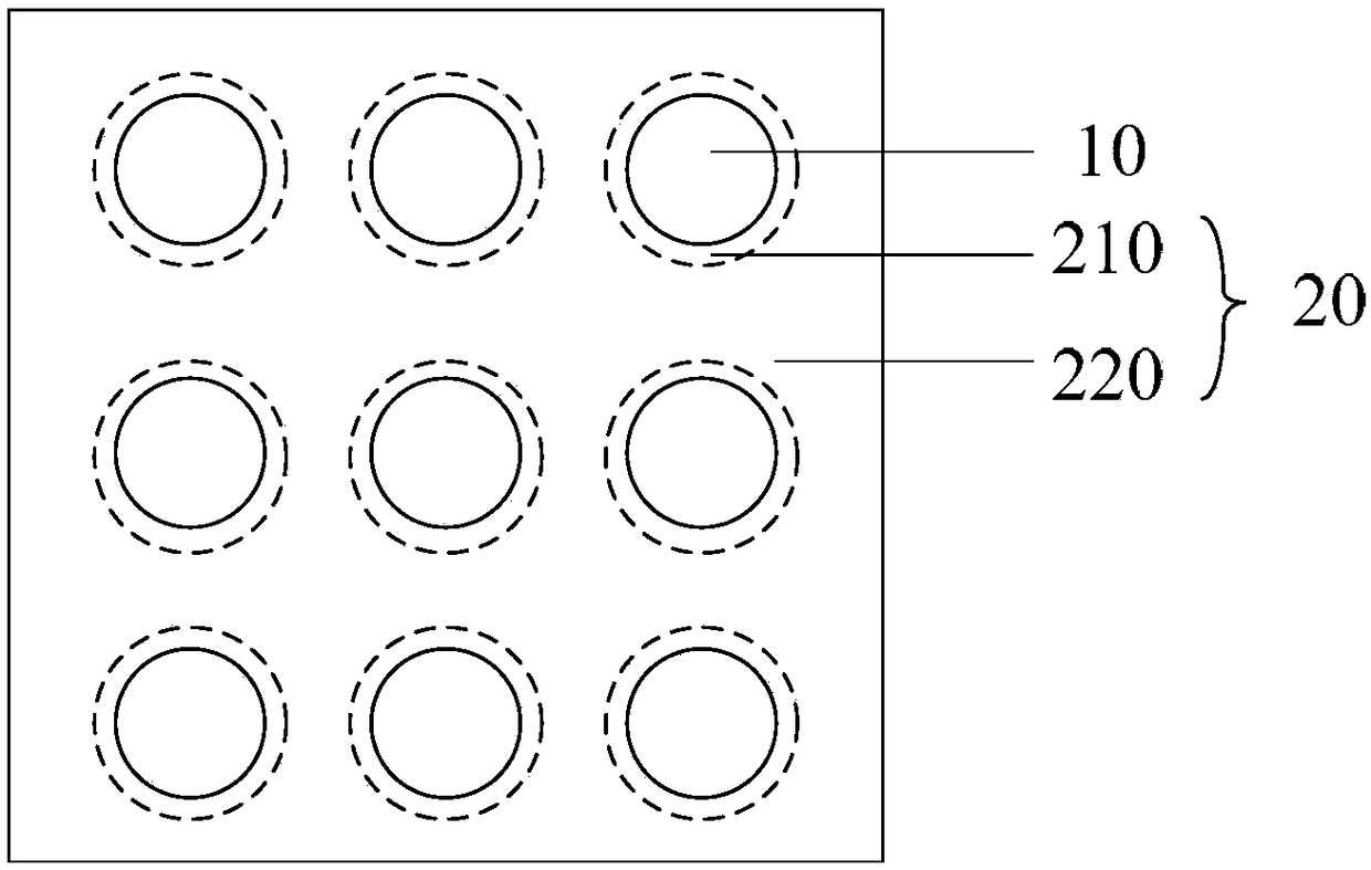
[0055] Step S1, placing a surface-modified mask on the first surface, and the surface-modified 96×64 hollowed-out parts correspond to one group of 96×64 microarray patterns in the hydrophobic region;
[0056] Step S2, using an inkjet printing (model Dimatix Materials Printer DMP-2831) process to make the hydrophobic red quantum dot ink enter the hydrophobic area through the hollow part;
[0057] Step S3, drying the quantum dot ink in the hydrophobic region,
[0058] Step S4, disposing the surface-modified mask on the first surface, and the surface-modified 96×64 hollowed-out parts correspond to another group of 96×64 microarray patterns in the hydrophobic region;
[0059] Step S5, using an inkjet printing (mod...
PUM
| Property | Measurement | Unit |
|---|---|---|
| boiling point | aaaaa | aaaaa |
Abstract
Description
Claims
Application Information
 - R&D
- Intellectual Property
- Life Sciences
- Materials
- Tech Scout
- Unparalleled Data Quality
- Higher Quality Content
- 60% Fewer Hallucinations
Browse by: Latest US Patents, China's latest patents, Technical Efficacy Thesaurus, Application Domain, Technology Topic, Popular Technical Reports.
© 2025 PatSnap. All rights reserved.Legal|Privacy policy|Modern Slavery Act Transparency Statement|Sitemap|About US| Contact US: help@patsnap.com