Semiconductor structure and forming method thereof

A semiconductor and gas technology, which is applied in the field of semiconductor structure and its formation, can solve the problems of uneven surface of the film, the influence of the protective effect of wafer devices, and the inability to smoothly grasp the wafer, so as to achieve the effect of improving reliability and protection

Active Publication Date: 2016-12-07
SEMICON MFG INT (SHANGHAI) CORP
View PDF7 Cites 2 Cited by
  • Summary
  • Abstract
  • Description
  • Claims
  • Application Information

AI Technical Summary

Problems solved by technology

[0005] However, in the prior art, in the process of attaching a film to the surface of the wafer, gas bulges often occur (please refer to figure 1 Medium gas bulging 10) makes the surface of the film uneven, so that in the subsequent process flow, the manipulator of the machine cannot smoothly grab the wafer, thereby affecting the transportation of the wafer, and the film that produces gas bulging is harmful to the wafer on the wafer. The protective effect of the device is also affected

Method used


Image

  • Semiconductor structure and forming method thereof
  • Semiconductor structure and forming method thereof
  • Semiconductor structure and forming method thereof

Examples


Embodiment Construction

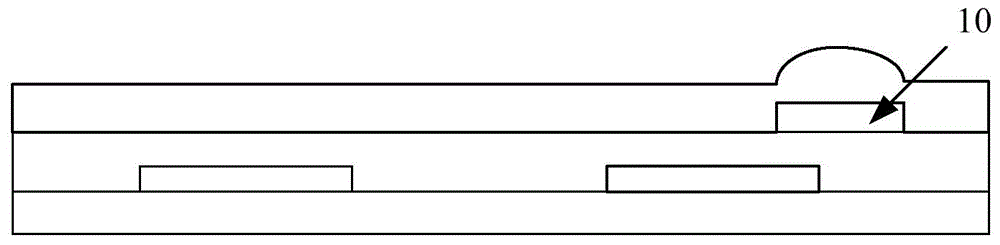
[0033] As mentioned in the background art, in the prior art, gas bulges are likely to be generated when the film is attached to the wafer surface, which affects the protective effect of the film, making it impossible for the machine to grasp the wafer smoothly in the subsequent process.

[0034] In the embodiment of the present invention, the protective film pasted on the substrate has a hole structure, which can discharge the gas, thereby avoiding the formation of gas bulges, ensuring the smoothness of the surface of the protective film, thereby improving the protection performance, and making the machine in the subsequent process smooth. Grab the substrate.

[0035] In order to make the above objects, features and advantages of the present invention more comprehensible, specific embodiments of the present invention will be described in detail below in conjunction with the accompanying drawings.

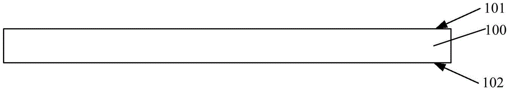
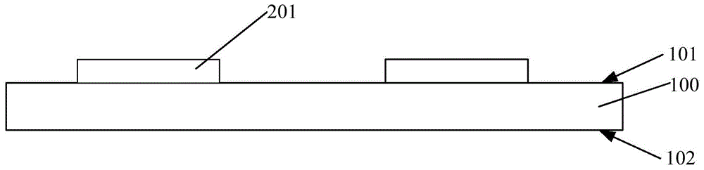
[0036] Please refer to figure 2 , providing a substrate 100 having a first su...


PUM

PropertyMeasurementUnit
diameteraaaaaaaaaa

Abstract

The invention relates to a semiconductor structure and a forming method thereof. The forming method for the semiconductor structure comprises the following steps of: providing a substrate, which is provided with a first surface and a second surface opposite to the first surface; forming a first device on the first surface of the substrate; forming a buffer layer covering the first surface of the substrate and the first device; and sticking a protective film on the surface of the buffer layer, wherein the protective film is provided with a hole structure; and the hole structure comprises multiple holes. By means of the forming method for the semiconductor structure, gas bump formed between the buffer layer and the protective film can be avoided; and the protection performance of the protective film and the reliability when the substrate is grabbed by a machine in a following process can be improved.

Description

technical field [0001] The invention relates to the technical field of semiconductors, in particular to a semiconductor structure and a forming method thereof. Background technique [0002] As an interdisciplinary advanced manufacturing technology originated in the 1990s, micro-electromechanical systems (MEMS) are widely used to improve people's quality of life, improve people's living standards and enhance national strength. MEMS is a technology that uses the micro-processing technology of semiconductor integrated circuits to integrate sensors, brakes, and control circuits on tiny chips, also known as micro-nano technology. At present, it has been widely used in communication, automobile, optics, biology and other fields. [0003] In some MEMS fields, in order to meet the functional requirements of the device, it is usually necessary to form devices on both the front and back sides of the wafer. Usually after the device is formed on one side of the wafer, the other side o...

Claims


Application Information

Patent Timeline
Patent Type & Authority Applications(China)
IPC IPC(8): B81C1/00B81B7/00
Inventor 郑超马军德王伟
Owner SEMICON MFG INT (SHANGHAI) CORP
Why Eureka
Try Eureka