
Color filter substrate and manufacturing method thereof and liquid crystal display panel

A color filter technology and a manufacturing method, which are applied in optics, nonlinear optics, instruments, etc., can solve problems such as high cost and complicated manufacturing process, and achieve the effects of reducing saturation voltage, simplifying process, and improving transmittance.

Inactive Publication Date: 2016-12-07
KUSN INFOVISION OPTOELECTRONICS
View PDF6 Cites 18 Cited by
  • Summary
  • Abstract
  • Description
  • Claims
  • Application Information

AI Technical Summary

Problems solved by technology

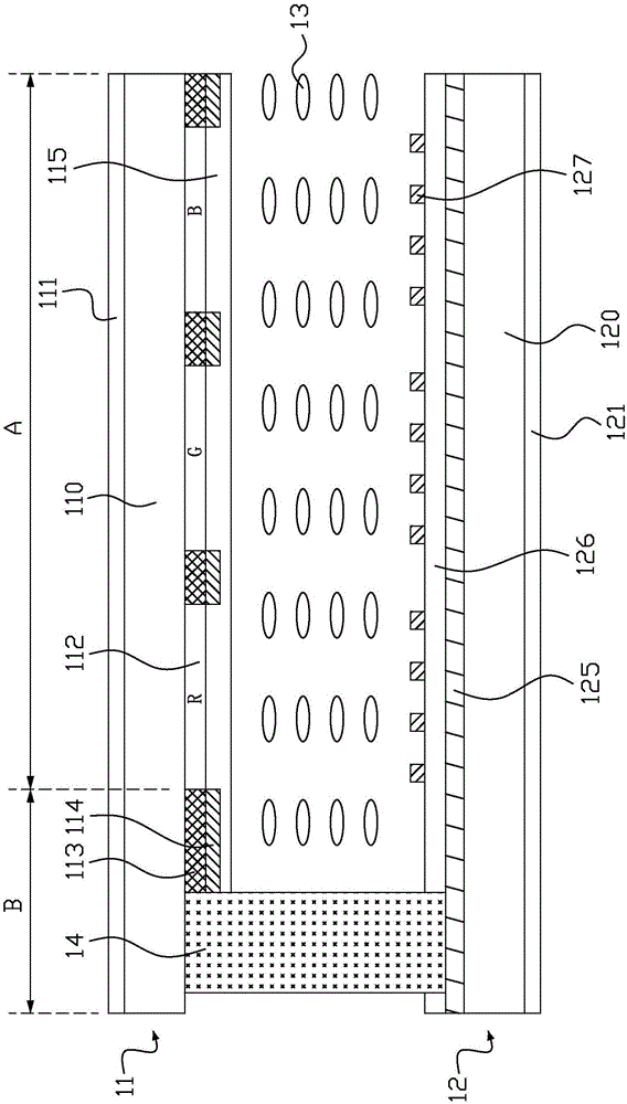
[0011] The purpose of the present invention is to provide a color filter substrate and a manufacturing method to solve the problems of complex manufacturing process, high cost, alignment and light leakage when the existing color filter substrate is provided with a shielding electrode

Method used


Image

  • Color filter substrate and manufacturing method thereof and liquid crystal display panel
  • Color filter substrate and manufacturing method thereof and liquid crystal display panel
  • Color filter substrate and manufacturing method thereof and liquid crystal display panel

Examples


Embodiment Construction

[0063] In order to further illustrate the technical methods and effects of the present invention to achieve the intended purpose of the invention, the specific implementation, structure, features and effects of the present invention will be described in detail below with reference to the drawings and embodiments.

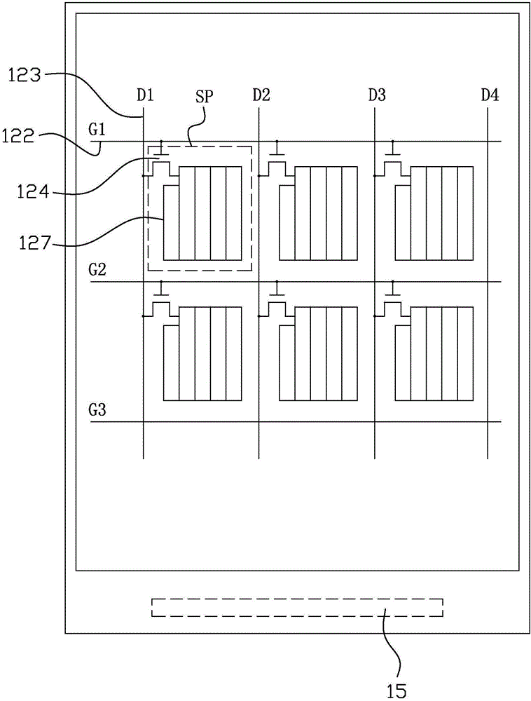
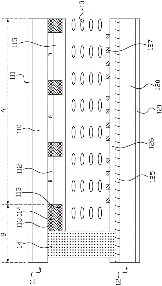
[0064] figure 1 It is a schematic diagram of the structure of the liquid crystal display panel in the first embodiment of the present invention, please refer to figure 1 The liquid crystal display panel includes a first substrate 11, a second substrate 12 disposed opposite to the first substrate 11, and a liquid crystal layer 13 located between the first substrate 11 and the second substrate 12. The first substrate 11 is a color filter substrate, and the second substrate 12 is a thin film transistor array substrate.

[0065] The liquid crystal display panel provided in this embodiment is suitable for in-plane switching (IPS), fringe electric field switching (FFS) and othe...


PUM


Abstract

The invention relates to a color filter substrate and a manufacturing method thereof and a liquid crystal display panel. The color filter substrate comprises a substrate, one side of which is provided with a color resistance layer, black matrixes and shielding electrodes made by conductive material. The color filter substrate is provided with a display area and a non-display area arranged on the periphery of the display area. The shielding electrodes and the black matrixes shared the same pattern in the display area and the non-display area. The shielding electrodes and the black matrixes are attached to each other and overlapped together.In the embodiment, a light cover is utilized for exposure such that the black matrixes and the shielding electrodes are made at the same time. Without adding the light cover for making the shielding electrodes, production cost is reduced and a contraposition problem is avoided. The shielding electrodes are conducted with public electrodes in an array substrate through conductive glue from the side surface of the shielding electrodes. Therefore, light leakage is avoided due to poor coating of a sealant.

Description

Technical field [0001] The present invention relates to the technical field of liquid crystal display, in particular to a color filter substrate, a manufacturing method and a liquid crystal display panel. Background technique [0002] Liquid crystal display panels (LCDs) have the advantages of good image quality, small size, light weight, low driving voltage, low power consumption, no radiation, and relatively low manufacturing costs, and are dominant in the field of flat panel displays. The liquid crystal display panel includes a color filter substrate, a thin film transistor array substrate and a liquid crystal layer sandwiched between them. [0003] Generally, when a user views the screen of the liquid crystal display panel from different viewing angles, the brightness of the image will decrease as the viewing angle increases. In a traditional twisted nematic (TN) liquid crystal display panel, the common electrode and the pixel electrode are formed on two different substrates, ...

Claims


Application Information

Patent Timeline
IPC IPC(8): G02F1/1335G02F1/1343
CPCG02F1/133512G02F1/133514G02F1/133516G02F1/134309
Inventor 钟德镇廖家德苏子芳黄丽玉
Owner KUSN INFOVISION OPTOELECTRONICS
Learn More