Device for detecting X-ray performance of semiconductor material

An X-ray and semiconductor technology, applied in the field of semiconductor material performance detection, can solve problems affecting detection accuracy, low current level, weak current detection interference, etc., and achieve the effect of reducing test cost, reducing interference, and convenient operation

Pending Publication Date: 2019-07-26
SUZHOU UNIV
View PDF0 Cites 1 Cited by
  • Summary
  • Abstract
  • Description
  • Claims
  • Application Information

AI Technical Summary

Problems solved by technology

However, since radiation detection requires a very low current level, the generated weak current detection is easily disturbed by factors such as the external environment, thus affecting the accuracy of detection

Method used


Image

  • Device for detecting X-ray performance of semiconductor material

Examples


Embodiment Construction

[0018] The present invention will be further described below in conjunction with the accompanying drawings and specific embodiments, so that those skilled in the art can better understand the present invention and implement it, but the examples given are not intended to limit the present invention.

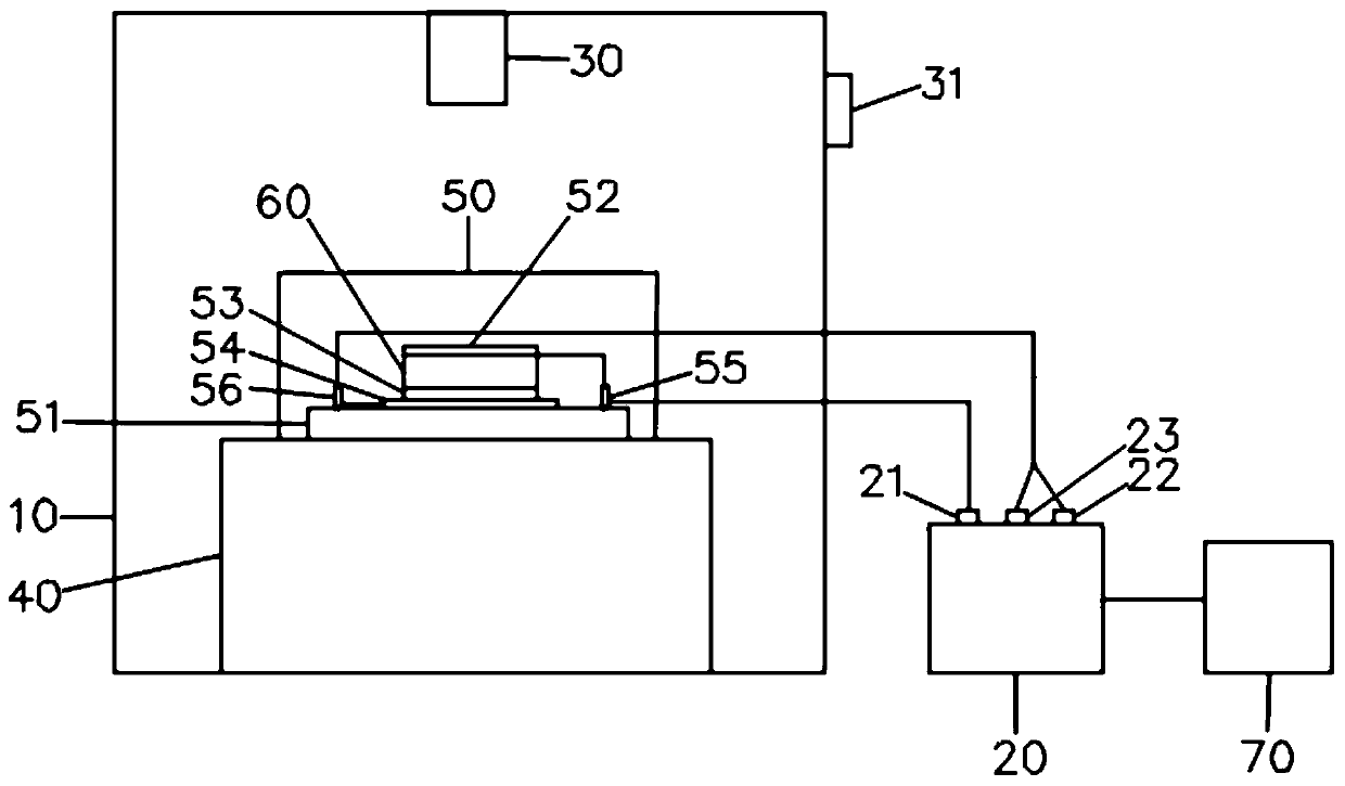
[0019] Based on the photoelectric response of the material, electrons and holes are generated in the semiconductor material under the irradiation of X-rays. Under the action of an external electric field, the electrons and holes will be separated. In the electric field circuit, electrons and holes will achieve directional migration, thereby generating a current signal.

[0020] like figure 1 Shown is a device for detecting X-ray properties of semiconductor materials in an embodiment of the present invention, and the device includes a dark box 10 and an electrometer 20 . In this embodiment, the electrometer 20 is a high resistance electrometer, preferably a KEIFHLEY 6517B high re...


PUM

PropertyMeasurementUnit
electrical resistivityaaaaaaaaaa

Abstract

The invention discloses a device for detecting the X-ray performance of a semiconductor material, which comprises a camera bellows and an electrometer, wherein an electromagnetic shielding box is arranged in the camera bellows; an opening is formed above the electromagnetic shielding box; an X-ray light source is arranged above the opening; a PCB board is arranged in the electromagnetic shieldingbox; a first conductive adhesive, a second conductive adhesive, a first pin and a second pin are arranged on the PCB board; the first conductive adhesive and the second conductive adhesive are respectively adhered to the upper surface and the lower surface of a sample; the first conductive adhesive is electrically connected with the first pin; the second conductive adhesive is electrically connected with the second pin; the first pin is connected with a high-voltage input port of the electrometer; and the second pin is connected with a signal input port of the electrometer. The device for detecting the X-ray performance of the semiconductor material is simple in structure and convenient to operate, can well realize electrostatic shielding, reduces interference of external environment on detection, and greatly reduces testing cost. Meanwhile, the connection among all the parts is stable, and the weak current of the sample can be accurately measured, so that the X-ray performance of thesample is obtained.

Description

technical field [0001] The invention relates to the technical field of semiconductor material performance detection, in particular to a device for detecting X-ray performance of semiconductor materials. Background technique [0002] Semiconductor materials are a class of electronic materials that have semiconductor properties (conductivity is between conductors and insulators, and resistivity is in the range of 1mΩ·cm~1GΩ·cm), and can be used to make semiconductor devices and integrated circuits. Semiconductor materials can directly absorb radioactive rays, and generate electron-hole pairs through photoelectric effect, Compton scattering, and electron pair generation. They move in an external electric field to generate the basic electrical signal of the detector. After the signal is collected, the corresponding switch ratio of the material can be obtained, the sensitivity of material detection can be calculated, and the μτ product of the material can be calculated. However,...

Claims


Application Information

Patent Timeline
Patent Type & Authority Applications(China)
IPC IPC(8): G01N23/00H05K9/00
CPCG01N23/00H05K9/002
Inventor 王殳凹陈兰花梁城瑜翟富万程丽葳王亚星
Owner SUZHOU UNIV
Why Eureka
Try Eureka