A kind of topological insulator thin film with photovoltaic properties and preparation method thereof
A technology of topological insulators and photovoltaic properties, applied in photovoltaic power generation, semiconductor/solid-state device manufacturing, semiconductor devices, etc., to achieve good solar cells and optoelectronic application prospects, low cost, and easy scale production
- Summary
- Abstract
- Description
- Claims
- Application Information
AI Technical Summary
Problems solved by technology
Method used
Image
Examples
Embodiment 1
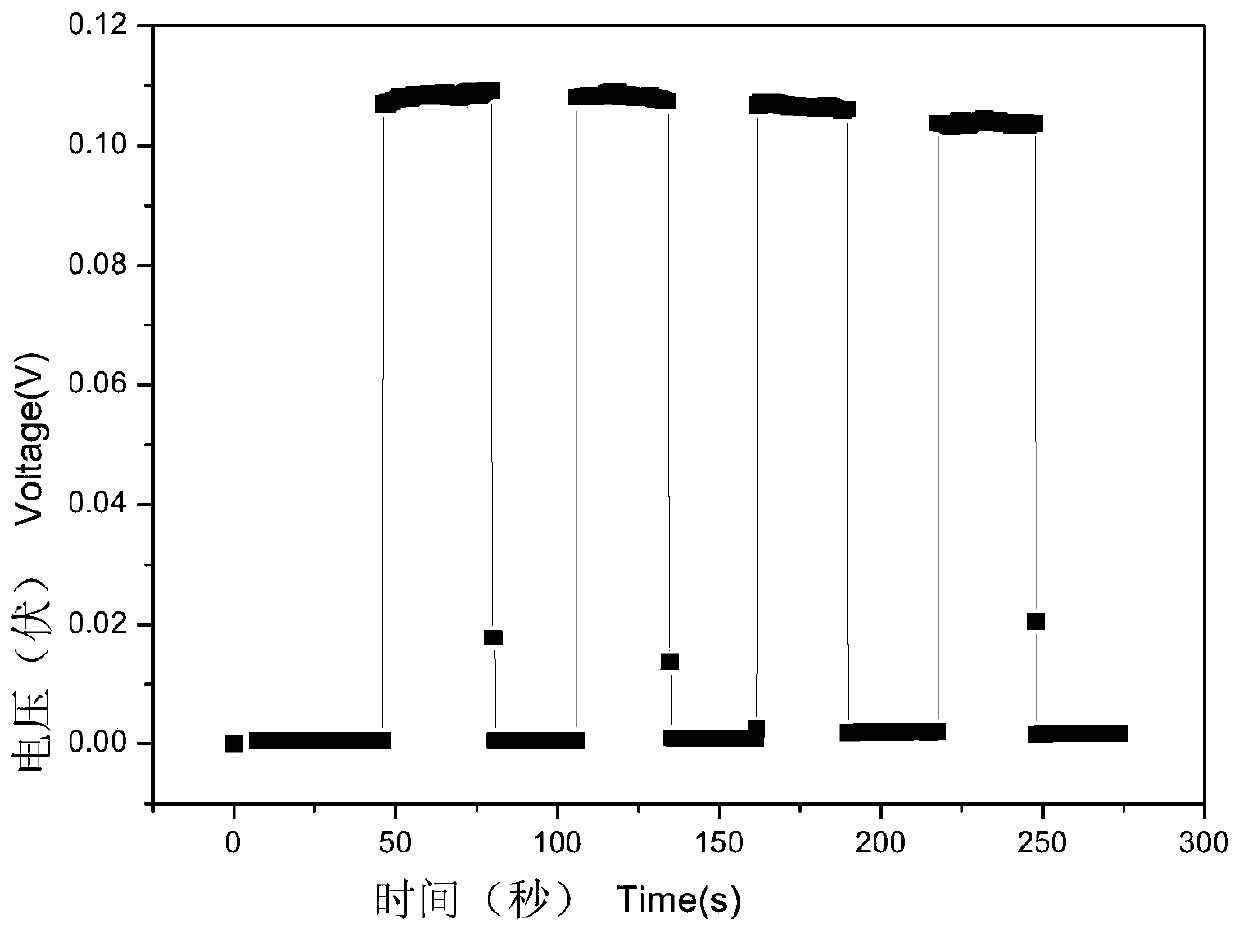
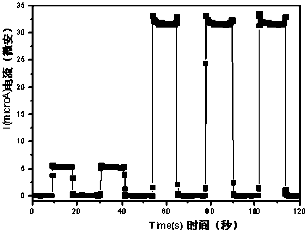
[0023] The bismuth telluride thin film is prepared by chemical vapor deposition method, the P-type silicon substrate is used as the substrate, and the substrate is treated with ethanol, acetone and dilute hydrofluoric acid successively. The raw material is bismuth telluride powder with a purity of 99.99%, the total gas flow rate is 50 sccm, and the volume ratio of argon to hydrogen is 4:1. The working pressure is 50Pa, the furnace center temperature is 520°C, the distance between the substrate and the furnace center is 14.5 cm, the substrate temperature is about 300°C, and the working time is 5 minutes. Using nanovoltmeter and sunlight to test the electrode potential and current-voltage curve of the thin film material in the light and dark state, all the tests are in the atmospheric state, let the sunlight directly shine on the film through the glass, which is close to the actual application situation, and the measured The open-circuit photovoltage of the thin film is 0.11V, a...
Embodiment 2
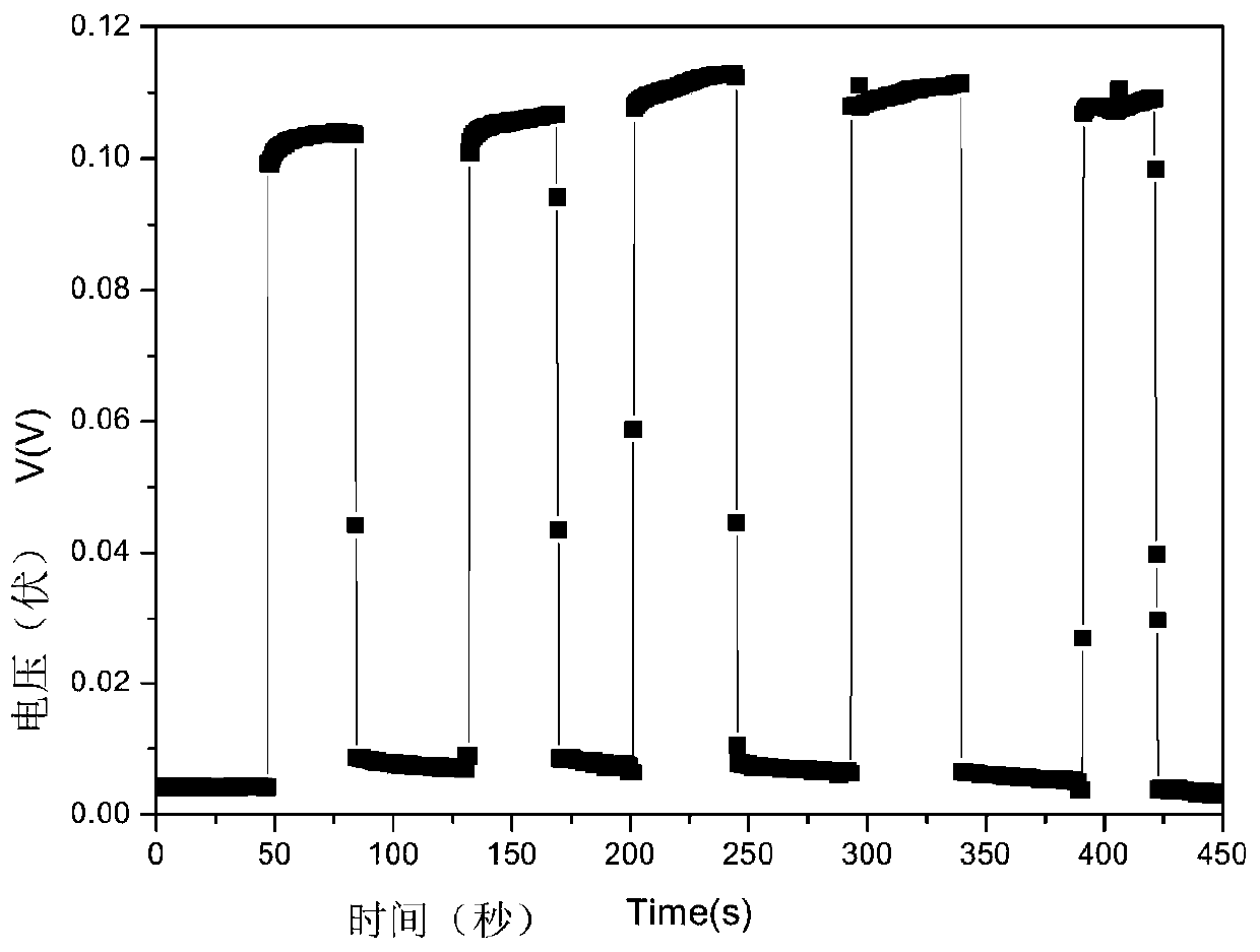
[0025] The bismuth selenide thin film is prepared by chemical vapor deposition method, the P-type silicon substrate is used as the substrate, and the substrate is treated with ethanol, acetone and dilute hydrofluoric acid successively. The raw material is bismuth selenide powder with a purity of 99.99%, the total gas flow rate is 50 sccm, and the volume ratio of argon to hydrogen is 4:1. The working pressure is 50Pa, the furnace center temperature is 520°C, the distance between the substrate and the furnace center is 14.5 cm, the substrate temperature is about 300°C, and the working time is 10 minutes. The measured photovoltage of the film is 0.11V, and its voltage changes with sunlight irradiation see image 3 .
Embodiment 3
[0027] The antimony telluride thin film is prepared by chemical vapor deposition method, the P-type silicon substrate is used as the substrate, and the substrate is treated with ethanol, acetone and dilute hydrofluoric acid successively. The raw material is antimony telluride powder with a purity of 99.99%. The distance between the substrate and the center of the furnace is 14.5 cm. The total gas flow rate is 50 sccm, and the volume ratio of argon to hydrogen is 4:1. The working pressure is 50Pa, the furnace center temperature is 520°C, and the working time is 5 minutes. The measured photovoltage of the film is 0.09V, and its voltage changes with sunlight irradiation see Figure 4 .
PUM
| Property | Measurement | Unit |
|---|---|---|
| thickness | aaaaa | aaaaa |
| size | aaaaa | aaaaa |
| size | aaaaa | aaaaa |
Abstract
Description
Claims
Application Information


