Chip package structure and manufacturing method thereof

A technology of chip packaging structure and manufacturing method, which is applied in semiconductor/solid-state device manufacturing, electrical components, electric solid-state devices, etc., can solve the problem of increasing the inner pin pitch, unable to increase the contact density of the chip packaging structure, and unable to achieve micro-pitch, etc. problem, to achieve the effect of increasing the contact density

Active Publication Date: 2016-12-07
CHIPMOS TECH INC
View PDF5 Cites 2 Cited by
  • Summary
  • Abstract
  • Description
  • Claims
  • Application Information

AI Technical Summary

Problems solved by technology

Although this can prevent the molten bumps from overflowing to the lower surface of the inner pins, it also increases the distance between any two adjacent inner pins, which cannot meet the requirement of fine pitch. It is also impossible to increase the contact density in the chip packaging structure

Method used


Image

  • Chip package structure and manufacturing method thereof
  • Chip package structure and manufacturing method thereof
  • Chip package structure and manufacturing method thereof

Examples


Embodiment Construction

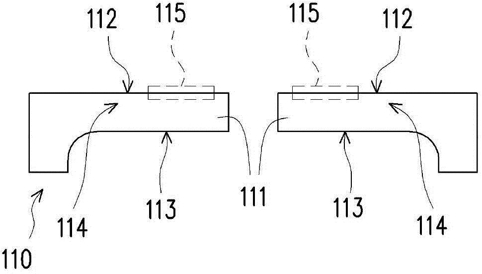
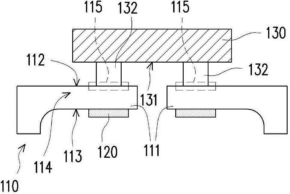
[0046] Figure 1A to Figure 1E It is a schematic diagram of the manufacturing process of the chip packaging structure according to an embodiment of the present invention. Figure 1F for Figure 1E A partial cross-sectional schematic diagram of the chip package structure along the section line A-A. First, please refer to Figure 1A , providing a lead frame 110 as a carrier. The lead frame 110 has a plurality of inner pins 111, wherein each inner pin 111 has an upper surface 112, a lower surface 113 opposite to the upper surface 112, and opposite side surfaces 114 connecting the upper surface 112 and the lower surface 113 (shown in Figure 1F ) and the bonding area 115 on the upper surface 112.

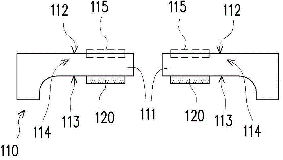
[0047] Next, please refer to Figure 1B A solder resist layer 120 is formed on the lower surface 113 of each inner lead 111 and at least corresponds to the bonding area 115 of each inner lead 111 . Specifically, the solder resist layer 120 is, for example, formed on the lower surfa...


PUM


Abstract

A chip package structure including a lead frame, a chip, a plurality of solder bumps, a solder resist layer and an encapsulant is provided. The lead frame has a plurality of inner leads. Each of the inner leads has an upper surface, a lower surface, two side surfaces opposite to each other and a bonding area on the upper surface. The chip is disposed on the lead frame and has an active surface. Each of the solder bumps connects the active surface and the bonding area of each of the inner leads. The solder resist layer is disposed on at least one of the lower surface or the two side surfaces of each of the inner leads. The encapsulant covers the lead frame, the chip, the solder bumps and the solder resist layer. A manufacturing method of the chip package structure is also provided.

Description

technical field [0001] The present invention relates to a packaging structure and its manufacturing method, and in particular to a chip packaging structure and its manufacturing method. Background technique [0002] In recent years, with the rapid development of electronic technology and the emergence of high-tech electronic industries, electronic products with more humanization and better functions are constantly being introduced, and are designed towards the trend of light, thin, short and small. As far as the chip packaging technology is concerned, each chip formed by dicing the wafer is disposed on a carrier by, for example, wire bonding or flip-chip bonding, wherein the aforementioned carrier can be a lead frame or a substrate. Taking the flip-chip packaging structure in the form of a lead frame as an example, the active surface of the chip faces the lead frame, and the chip is bonded to the lead frame through a plurality of bumps on the active surface or on the leads o...

Claims


Application Information

Patent Timeline
Patent Type & Authority Applications(China)
IPC IPC(8): H01L23/31H01L21/58H01L21/56
CPCH01L23/3107H01L23/4951H01L23/49548H01L23/49582H01L24/13H01L24/16H01L24/81H01L2224/10175H01L2224/13109H01L2224/13111H01L2224/13113H01L2224/13118H01L2224/1312H01L2224/13139H01L2224/13147H01L2224/13155H01L2224/16013H01L2224/1607H01L2224/16245H01L2224/81439H01L2224/81455H01L2224/81464H01L2224/81466H01L2224/81469H01L2224/81484H01L2224/81815H01L2924/181H01L2924/00012H01L2924/00014H01L2924/014H01L2924/013H01L2924/01074H01L2924/01022H01L24/00H01L2021/60022
Inventor 石智仁
Owner CHIPMOS TECH INC
Why Eureka
Try Eureka