Display panel reduction method and display device

A display panel and display device technology, which is applied in the manufacture of electrical components, electrical solid devices, semiconductor/solid device, etc., can solve the problems of actual effect influence, influence on display effect, uneven display surface of display panel, etc.

Inactive Publication Date: 2016-12-14
BOE TECH GRP CO LTD +1
View PDF4 Cites 8 Cited by
  • Summary
  • Abstract
  • Description
  • Claims
  • Application Information

AI Technical Summary

Problems solved by technology

In the process steps before chemical thinning, tiny recessed structures 1 (such as Figure 1a As shown), its opening and depth are several microns; when the subsequent thinning process is performed, the recessed structure 1 will become larger after being etched by

Method used


Image

  • Display panel reduction method and display device
  • Display panel reduction method and display device
  • Display panel reduction method and display device

Examples


Embodiment Construction

[0030] Specific embodiments of the present invention will be described in detail below in conjunction with the accompanying drawings. It should be understood that the specific embodiments described here are only used to illustrate and explain the present invention, not to limit the present invention.

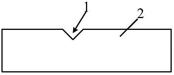
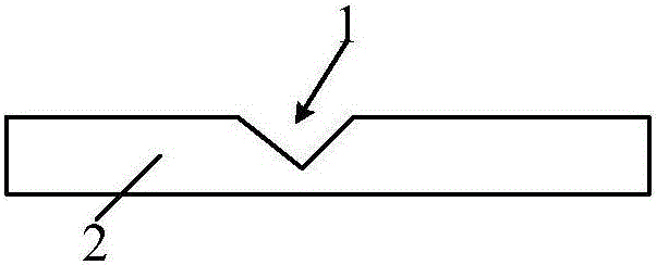
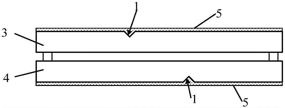
[0031] As an aspect of the present invention, a method for thinning a display panel is provided, such as Figure 2a As shown, the display panel includes an array substrate 4 and a box-facing substrate 3 arranged opposite to the box, and a plurality of recessed structures 1 (that is, tiny grooves) are formed on the surfaces of the array substrate 4 and the box-facing substrate 3 facing away from each other. . Such as image 3 As shown, the thinning method includes:

[0032] S1. Perform at least pretreatment on the paired cell substrate 3 . The pretreatment includes: forming a protective layer 5 on the surface formed with the recessed structure 1, so that the recessed structur...


PUM

PropertyMeasurementUnit
Thicknessaaaaaaaaaa

Abstract

The present invention provides a display panel reduction method. The display panel comprises an array substrate with the paired box arrangement and a paired box substrate, and the array substrate and the surface departing from the paired box substrate both have a plurality of depression structures. The reduction method comprises: at least performing preprocessing of the paired box substrate; and employing an etching liquid to perform etching of the paired box substrate and the surface departing from the array substrate. The preprocessing comprises: forming protective layers on the surfaces of the depression structures to allow the depression structures to be filled with the protective layers; forming the protective layers by using materials which cannot be etched by the etching liquid; and removing the portions of the protective layers located out of the depression structures, and retaining the portions of the protective layers located in the depression structures. Correspondingly, the present invention further provides a display device. The display panel reduction method and the display device can improve the display effect while realizing the panel thinness.

Description

technical field [0001] The invention relates to the field of display technology, in particular to a method for thinning a display panel and a display device. Background technique [0002] At present, in the production process of the display device, the upper and lower substrates of the display panel are usually subjected to a slimming process to obtain an ultra-thin display panel, and the viewing angle range can be enlarged after the thickness of the upper substrate is thinned. At present, etching solutions such as concentrated sulfuric acid and hydrofluoric acid are often used to react with the substrate for chemical thinning. In the process steps before chemical thinning, tiny recessed structures 1 (such as Figure 1a As shown), its opening and depth are several microns; when the subsequent thinning process is performed, the recessed structure 1 will become larger after being etched by the etching solution (such as Figure 1b As shown), this leads to the unevenness of the...

Claims


Application Information

Patent Timeline
IPC IPC(8): H01L21/77H01L27/12
CPCH01L27/1259
Inventor 彭艳召孟维欣郭建陈强任伟李亮黎文秀夏高飞
Owner BOE TECH GRP CO LTD
Why Eureka
Try Eureka