
Ball planting process and structure

A process and ball-mounting technology, applied in the direction of semiconductor/solid-state device components, semiconductor devices, electrical components, etc., can solve the problems of wafer gap, wafer surface bumps can not be turned on, and achieve the effect of ensuring reliability

Active Publication Date: 2019-01-04
NAT CENT FOR ADVANCED PACKAGING CO LTD
View PDF4 Cites 0 Cited by
  • Summary
  • Abstract
  • Description
  • Claims
  • Application Information

AI Technical Summary

Problems solved by technology

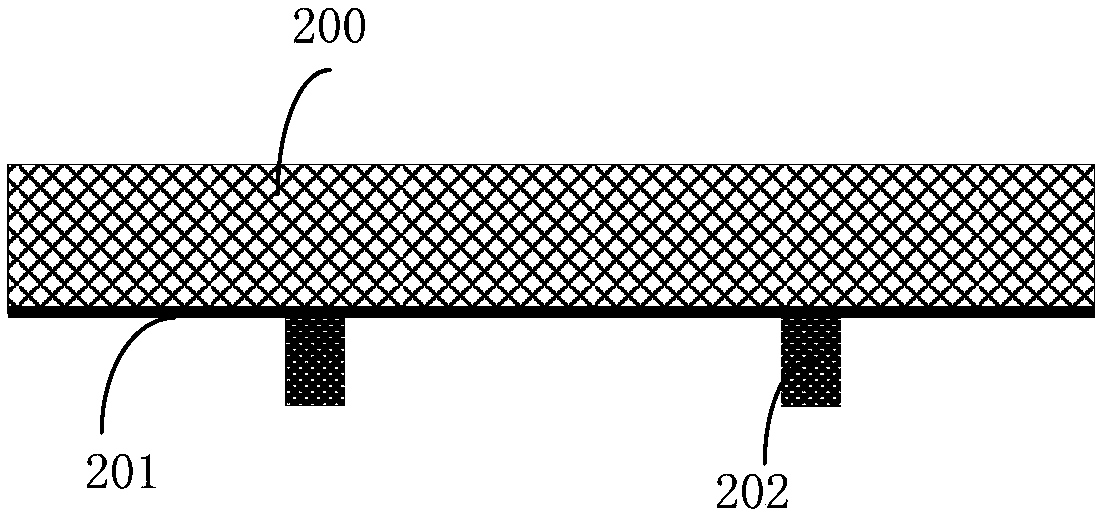
[0006] In view of the above-mentioned and / or existing problems in the existing semiconductor packaging bonding process that there is a gap between the wafers and the bumps on the surface of the wafer cannot be conducted, the present invention is proposed

Method used

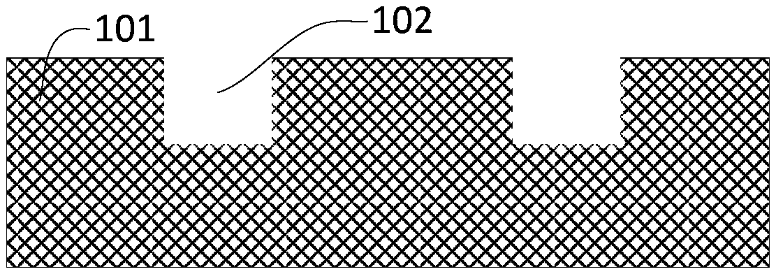
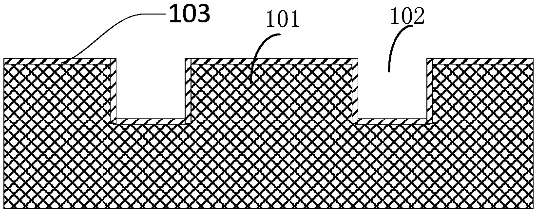

Image

  • Ball planting process and structure
  • Ball planting process and structure
  • Ball planting process and structure

Examples


Embodiment Construction

[0041] In order to make the above objects, features and advantages of the present invention more comprehensible, the specific implementation manners of the present invention will be further described below in conjunction with specific drawings.

[0042] In the following description, a lot of specific details are set forth in order to fully understand the present invention, but the present invention can also be implemented in other ways that are different from those described here, and those skilled in the art can do so without departing from the connotation of the present invention. By analogy, the present invention is not limited by the specific examples disclosed below.

[0043] Secondly, the present invention is described in detail in combination with schematic diagrams. When describing the embodiments of the present invention in detail, for the convenience of explanation, the cross-sectional view showing the device structure will not be partially enlarged according to the g...


PUM


Abstract

The invention discloses a ball mounting process and structure. The structure is characterized by comprising an upper wafer and a lower wafer, an upper wafer insulating layer is deposited on the lower surface of the upper wafer, and an insulating layer is deposited on the upper surface of the lower wafer; salient points are formed on the lower surface of the upper wafer, and the upper surface of the lower wafer is provided with embedded solder balls embedded into the upper surface of the lower wafer; the salient points on the lower surface of the upper wafer are embedded into the embedded solder balls of the lower wafer, and the bonding of the upper wafer insulating layer with the insulating layer on the upper surface of the lower wafer is realized. The embedded solder balls are arranged in embedding holes in the upper surface of the lower wafer, and the inner wall of each embedding hole is orderly provided with the insulating layer, a seed layer and a bonding pad layer, and the solder balls are arranged on the bonding pad layers of the embedding holes. The shapes and sizes of the embedding holes are consistent with the shapes and sizes of the salient points. Through the adoption of the process disclosed by the invention, the valid interconnection of the salient points of the wafer and the bonding reliability between two wafers can be guaranteed.

Description

technical field [0001] The invention relates to a ball planting process and structure, belonging to the technical field of semiconductors. Background technique [0002] With the development of semiconductor technology, the feature size of integrated circuits continues to shrink, and the interconnection density of devices continues to increase. Therefore, wafer-level packaging (Wafer Level Package, WLP) has gradually replaced wire-bonding packaging and has become a more commonly used packaging method. Wafer Level Packaging (WLP) technology is a technology that performs packaging and testing on the entire wafer and then cuts it to obtain a single finished chip. Requirements for lightness, smallness, shortness, thinning and low price. [0003] Both MEMS and CIS BSI processes in wafer-level packaging require bonding. Bonding processes are generally divided into anodic bonding, metal fusion bonding, and silicon oxide direct bonding. After bonding, the wafer is thinned, and the...

Claims


Application Information

Patent Timeline
Patent Type & Authority Patents(China)
IPC IPC(8): H01L23/488H01L21/60
CPCH01L24/13H01L24/16H01L24/81H01L2224/13H01L2224/16H01L2224/8119H01L2224/11
Inventor 姚波
Owner NAT CENT FOR ADVANCED PACKAGING CO LTD
Learn More