Cutting device

A cutting device and tape cutting technology, which is applied to fine working devices, stone processing tools, working accessories, etc., can solve the problems of troublesome adjustment, imperfect segmentation, damage to the surface of the substrate, etc., and achieve reliable and effective segmentation.

Active Publication Date: 2017-01-04
MITSUBOSHI DIAMOND IND CO LTD
View PDF11 Cites 3 Cited by
  • Summary
  • Abstract
  • Description
  • Claims
  • Application Information

AI Technical Summary

Problems solved by technology

[0011] When dividing with a cutting bar, if the pressing amount of the cutting bar into the substrate is large, the bending of the substrate will increase and the edges of the split ends will come into contact with each other, resulting in chipping at the split end face, or damage to the protective film. Substrate surface
Also, on the contrary, if the amount of pressing is small, problems such as undivided parts will occur due to insufficient bending of the substrate, so it is necessary to ensure an appropriate amount of pressing for cutting the strip.
[0012] However, the appropriate range of the above press-in a

Method used


Image

  • Cutting device
  • Cutting device
  • Cutting device

Examples


Example Embodiment

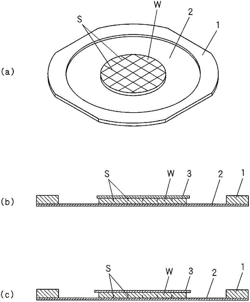
[0030] Hereinafter, the present invention will be described in detail based on the embodiments shown in the drawings. The semiconductor substrate W to be processed in this embodiment is mainly a semiconductor substrate for image sensors, and its form is similar to that described previously. figure 1 The semiconductor substrates shown are the same. Below, right figure 1 The cutting of the semiconductor substrate W in (c) will be described.
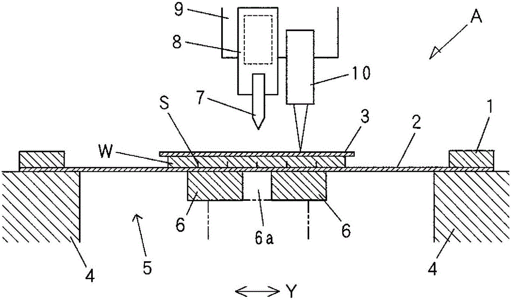
[0031] figure 2 It is an explanatory view showing the cutting mechanism part of the cutting device A of the present invention, and has a table 4 on which the semiconductor substrate W is placed together with the cutting frame 1. A space 5 is provided in the middle of the table 4, and a pair of left and right passive knives 6 and 6 are arranged in this space 5. The gap 6a formed between the passive knives 6, 6 is figure 2 It extends in the front-rear direction (X direction), and a long plate-shaped cutting strip 7 extending in the X directio...


PUM


Abstract

According to the present invention, there is provided a cutting device capable of maintaining an appropriate indentation amount of a cutting bar without being affected by the thickness of a semiconductor substrate, a protective film, and a dicing tape. The cutting device presses the cutting bar (7) into a semiconductor substrate (W) having a scribe line (S) on the surface to divide the substrate, one side of the semiconductor substrate (W) is covered with a protective film (3), and a dicing tape (2) is attached to the opposite side. The structure of the cutting device includes a workbench (4) for placing the semiconductor substrate (W) together with the protective film (3) and the dicing tape (2); a displacement gauge (10) for measuring the surface height of the protective film (3) or the dicing tape (2) placed on the upper surface side of the semiconductor substrate (W) of the workbench (4), and a computer (C) control part (11) that subtracts the displacement amount to the specified indentation amount of the cutting bar (7) to enable the cutting bar (7) to be lifted and lowered under the condition that the measured value obtained by the displacement gauge (10) has displacement relative to the pressing starting position of the cutting bar (7).

Description

technical field [0001] The invention relates to a cutting device for a semiconductor substrate made of brittle materials such as glass, silicon and ceramics. In particular, the present invention relates to a cutting device for cutting out unit products such as chips by dividing a semiconductor substrate along scribe lines processed on its surface. Background technique [0002] Usually, in the process of cutting out chips from a semiconductor substrate as a mother board, first, a knife wheel and a laser are used to scribe along a predetermined scribe line on the surface of the semiconductor substrate, thereby forming mutually orthogonal X and Y directions. Score lines (cracks). Thereafter, the semiconductor substrate is divided into square chips by pressing the cutting bar from the surface opposite to the scribed line with a cutting device to bend the substrate (see Patent Document 1 and Patent Document 2). [0003] Such as figure 1 As shown in (a), semiconductor substrate...

Claims


Application Information

Patent Timeline
IPC IPC(8): B28D1/22B28D5/04B28D7/00
CPCB28D1/22B28D5/0058B28D5/0064B28D5/04B28D7/00B28D7/005
Inventor 栗山规由武田真和村上健二桥本多市
Owner MITSUBOSHI DIAMOND IND CO LTD
Why Eureka
Try Eureka