Supercharge Your Innovation With Domain-Expert AI Agents!

Slave processing chip upgrade method and device

A technology for processing chips and chips, which is applied in the field of upgrading from processing chips, which can solve the problems that the improvement of image quality cannot be upgraded through software, the back-end image quality processing chip cannot be upgraded, and problems occur in TVs, so as to avoid improper upgrades and improve The effect of success rate and time cost reduction

Inactive Publication Date: 2017-01-04
HISENSE VISUAL TECH CO LTD
View PDF5 Cites 14 Cited by
  • Summary
  • Abstract
  • Description
  • Claims
  • Application Information

AI Technical Summary

Problems solved by technology

[0004] After the TV leaves the factory, it will not be possible to perform large-scale software upgrades on the back-end image quality processing chips, etc., or use the Internet to complete software upgrades by users themselves. The way to upgrade is to improve the TVs that have already left the factory
Due to the particularity of the back-end picture quality processing chip, once the upgrade fails, after-sales maintenance personnel need to remove the back cover of the TV for repair, which requires a lot of labor costs; and OTA upgrade is a large-scale upgrade method. Failure will cause a large number of TVs to have problems, which will lead to disastrous consequences, so there must be safety measures for the OTA upgrade of the back-end image quality processing chip

Method used


Image

  • Slave processing chip upgrade method and device
  • Slave processing chip upgrade method and device
  • Slave processing chip upgrade method and device

Examples


no. 1 example

[0051] Figure 4 It is a schematic diagram of the circuit principle of the first embodiment. It does not require the software carrier of the slave processing chip, so it has a wide range of applications.

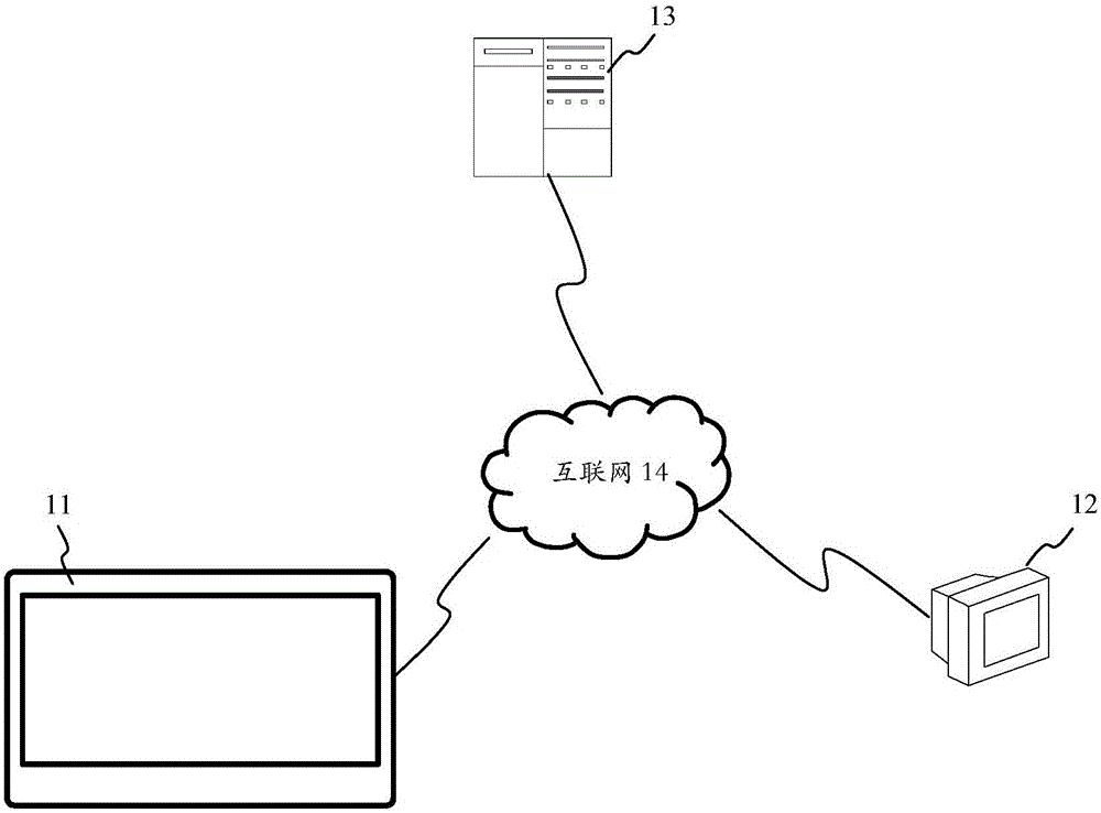
[0052] refer to Figure 4 The specific circuit of the upgrading device 11 may include: a master SOC, one or more network interface modules of the master SOC, one or more slave processing chips and their software carriers.

[0053] Both the main SOC and the slave processing chips that need software upgrades include I2C interfaces, and they are connected through the I2C bus laid out on the circuit board.

[0054] The slave processing chip software carrier adopts NORFlash without I2C interface, and the slave processing chip is connected to the corresponding NORFlash through the SPI interface. Each slave processing chip has only one NORFlash. In this embodiment, only one secondary processing chip needs to be upgraded: the back-end image quality processing chip.

[0055] SPI...

no. 2 example

[0085] Image 6 It is a schematic diagram of the circuit principle of the second embodiment. It requires that the software carrier of the slave processing chip must have an I2C interface, so that the scope of application is narrow but the control is simple and the efficiency is high.

[0086] refer to Image 6 Specifically, the specific circuit of the upgrading device 11 may include: a master SOC, one or more network interface modules of the master SOC, one or more slave processing chips and their software carriers.

[0087] The main SOC, the slave processing chip requiring software upgrade and the corresponding slave processing chip software carrier all include I2C interfaces, and they are connected through the I2C bus laid on the circuit board.

[0088] The software carrier of the slave processing chip adopts NORFlash with I2C interface, and the slave processing chip and the corresponding NORFlash are still connected through the SPI interface. Each slave processing chip h...


PUM


Abstract

The invention relates to a method and device for receiving and maintaining a program by applying internal storage of process equipment, in particular to a salve processing chip upgrade method and device with the function of verifying the accuracy of an upgrade program. The slave processing chip upgrade method comprises the steps that an upgrade software package is obtained through a main system level chip; the upgrade software package is loaded into a first booting area of a salve processing chip carrier, wherein the first booting area comprises a currently adopted slave processing chip main program; the upgrade software package of the first booting area is verified, a first check code is generated, and whether the first check code is correct or not is judged; if yes, upgrading is conducted, and if not, upgrading is not conducted. According to the method, the effect that due to inspection on the upgrade data package before upgrading, the probability of failed upgrading caused by data errors or incompleteness of the upgrade data package before upgrading is decreased and the function that after upgrading fails, normal booting for upgrading can be conducted again is achieved.

Description

technical field [0001] The invention relates to a method and a device for receiving and maintaining a program using the internal storage of a processing device, in particular to a method and device for upgrading from a processing chip with the ability to verify the accuracy of the upgrading program. Background technique [0002] In a smart device, in addition to the main system-on-chip (SOC) chip, there will also be a slave processing chip that shares part of the functions of the main SOC chip. Due to the high risk of upgrading the secondary processing chip and the inability to actively restore the original driver software after the upgrade fails, the secondary processing chip is generally not set to be actively upgraded. In order to avoid control confusion and system risk, the main SOC chip and the slave processing chip generally can only control their own peripheral components, but cannot directly control other peripheral components. Since the main SOC chip cannot directl...

Claims


Application Information

Patent Timeline
IPC IPC(8): G06F9/445
CPCG06F8/65
Inventor 李洋孙进伟陈世雷曾小光
Owner HISENSE VISUAL TECH CO LTD
Features
  • R&D
  • Intellectual Property
  • Life Sciences
  • Materials
  • Tech Scout
  • Unparalleled Data Quality
  • Higher Quality Content
  • 60% Fewer Hallucinations
Learn More