Chip debugging method and device
A debugging method and chip technology, applied in the electronic field, can solve problems such as high cost and limited functions, and achieve the effect of low cost, reduced cost and rich functions
- Summary
- Abstract
- Description
- Claims
- Application Information
AI Technical Summary
Problems solved by technology
Method used
Image


Examples
Embodiment 1
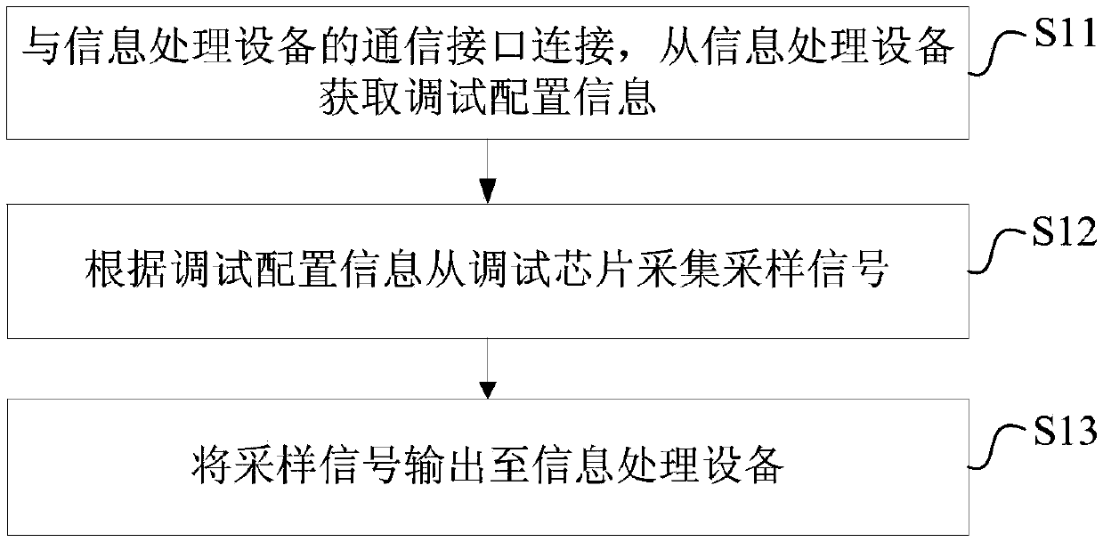
[0052] refer to figure 1 , propose the chip debugging method of the first embodiment of the present invention, described method comprises the following steps:
[0053] S11. Connect to the communication interface of the information processing device, and acquire debugging configuration information from the information processing device.
[0054] The chip debugging device is connected with the communication interface of the information processing equipment, and communicates through the communication interface. Optionally, the chip debugging device and the information processing device may communicate through the Joint Test Action Group (JTAG) protocol. In this case, the communication interface of the information processing device needs to be converted into the JTAG protocol. Among them, the parallel port is a common, standard, and simple interface, and the hardware connection is simple, and the driver development is also simple. Users can develop drivers and upper-layer applica...
Embodiment 2
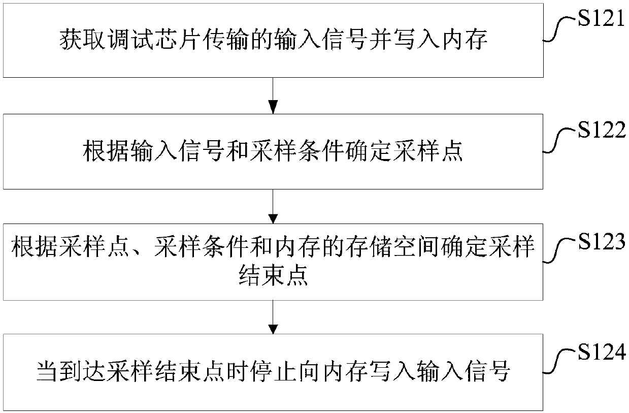
[0091] refer to Figure 7 , the chip debugging device of the second embodiment of the present invention is proposed, the device includes an interface control module and a signal acquisition module, wherein:
[0092] Interface control module: used to connect with the communication interface of the information processing device, obtain debugging configuration information from the information processing device, and output the sampling signal collected by the signal acquisition module to the information processing device.
[0093] The interface control module is connected with the communication interface of the information processing device, and communicates through the communication interface. Optionally, the interface control module and the information processing device can communicate through the Joint Test Action Group (JTAG) protocol. At this time, the communication interface of the information processing device needs to be converted into the JTAG protocol. The timing interf...
PUM
 Abstract
Description
Claims
Application Information
 - R&D
- Intellectual Property
- Life Sciences
- Materials
- Tech Scout
- Unparalleled Data Quality
- Higher Quality Content
- 60% Fewer Hallucinations
Browse by: Latest US Patents, China's latest patents, Technical Efficacy Thesaurus, Application Domain, Technology Topic, Popular Technical Reports.
© 2025 PatSnap. All rights reserved.Legal|Privacy policy|Modern Slavery Act Transparency Statement|Sitemap|About US| Contact US: help@patsnap.com