

Semiconductor structure forming method
A technology of semiconductor and gate structure, which is applied in the field of formation of semiconductor structures, and can solve the problems of increased difficulty in the process of fin field effect transistors and unstable performance of fin field effect transistors.
- Summary
- Abstract
- Description
- Claims
- Application Information
AI Technical Summary
Problems solved by technology
Method used
Image

Examples
Embodiment Construction
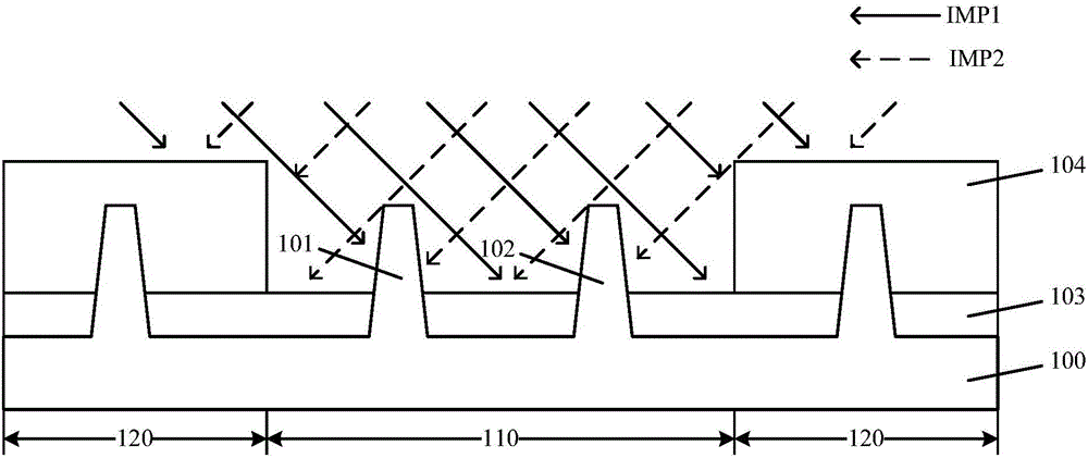
[0032] As mentioned in the background, with the reduction of the size of semiconductor devices and the increase of device density, the difficulty of forming the fin field effect transistor increases, and the performance of the formed fin field effect transistor is also unstable.
[0033] After research, it is found that for fin field effect transistors, the fins are used as active regions, and after the gate structure is formed on the surface of the fins, it is necessary to form an ion implantation process in the fins on both sides of the gate structure. lightly doped region. Since the part of the sidewall and top of the fin covered by the gate structure is used to form a channel region, the formed lightly doped region also needs to cover the sidewall and top of the fin, thus it is necessary to use Ion implantation processes with different angles perform light dopant implantation on the sidewalls and tops of several fins respectively. However, due to the different angles of t...
PUM
| Property | Measurement | Unit |
|---|---|---|
| Thickness | aaaaa | aaaaa |
Abstract
Description
Claims
Application Information