A preparation method and system of phosphor copper anode for integrated circuit

An integrated circuit and phosphor copper technology, which is applied in the field of preparation of phosphor copper anodes for integrated circuits, can solve the problems of complex manufacturing process, etc., and achieve the effects of simple manufacturing process, high ductility, and high filling capacity.

Active Publication Date: 2019-01-22
佛山市承安集团股份有限公司
View PDF6 Cites 0 Cited by
  • Summary
  • Abstract
  • Description
  • Claims
  • Application Information

AI Technical Summary

Problems solved by technology

[0003] Chinese patent 201010581922.8 discloses a method for preparing phosphor copper anodes for integrated circuits. High-purity graphite is used as crucible and mold materials, and high-purity copper ingots with a purity of 99.99% and above are melted in a high-vacuum intermediate-frequency induction melting furnace. Add phosphorus-bronze master alloy containing 6-16wt.% phosphorus at 1150-1300°C, add phosphor-bronze master alloy to high-purity copper ingot with a weight ratio of 1:50-600, and keep warm at 1150-1300°C for 20-30min , after standing still for 20 minutes, pouring into graphite molds to obtain phosphor-bronze alloy ingots; the obtained phosphor-bronze alloy ingots were cut off the risers of the ingots, then multi-directional forged and rolled, and kept at 300-600°C for 0.5 After ~12 hours of recrystallization treatment, after surface treatment, the phosphor copper anode for integrated circuits is machined, but this manufacturing process is still complicated

Method used


Image

  • A preparation method and system of phosphor copper anode for integrated circuit
  • A preparation method and system of phosphor copper anode for integrated circuit
  • A preparation method and system of phosphor copper anode for integrated circuit

Examples


Embodiment Construction

[0030] In order to fully understand the technical content of the present invention, the technical solutions of the present invention will be further introduced and illustrated below in conjunction with specific examples, but not limited thereto.

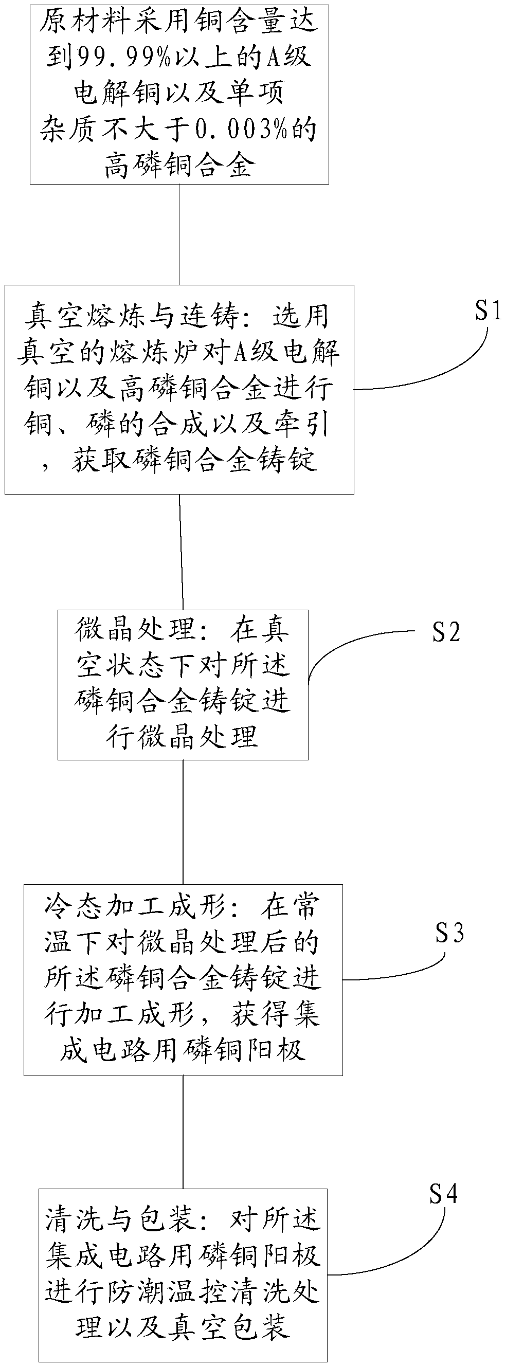
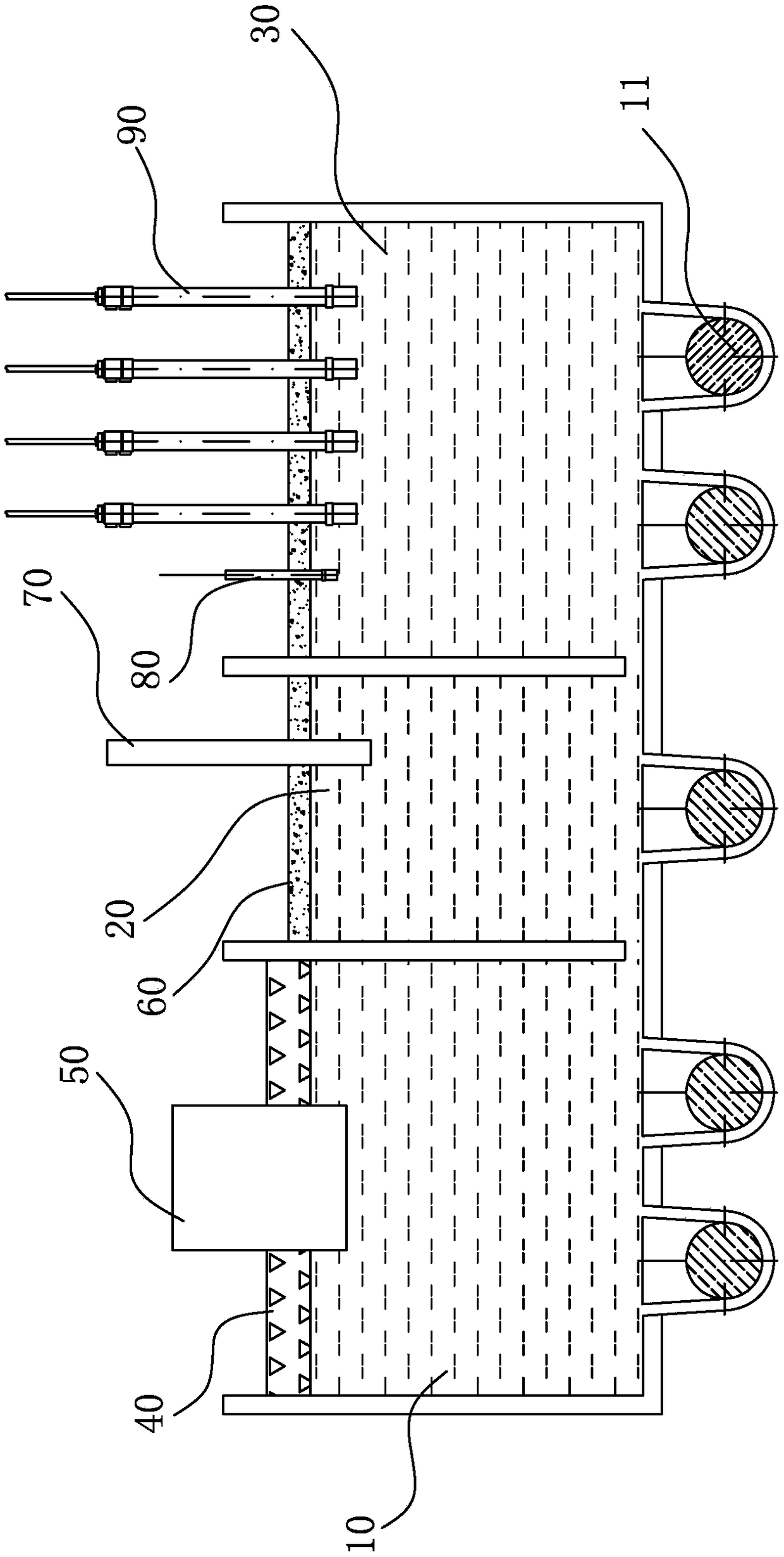
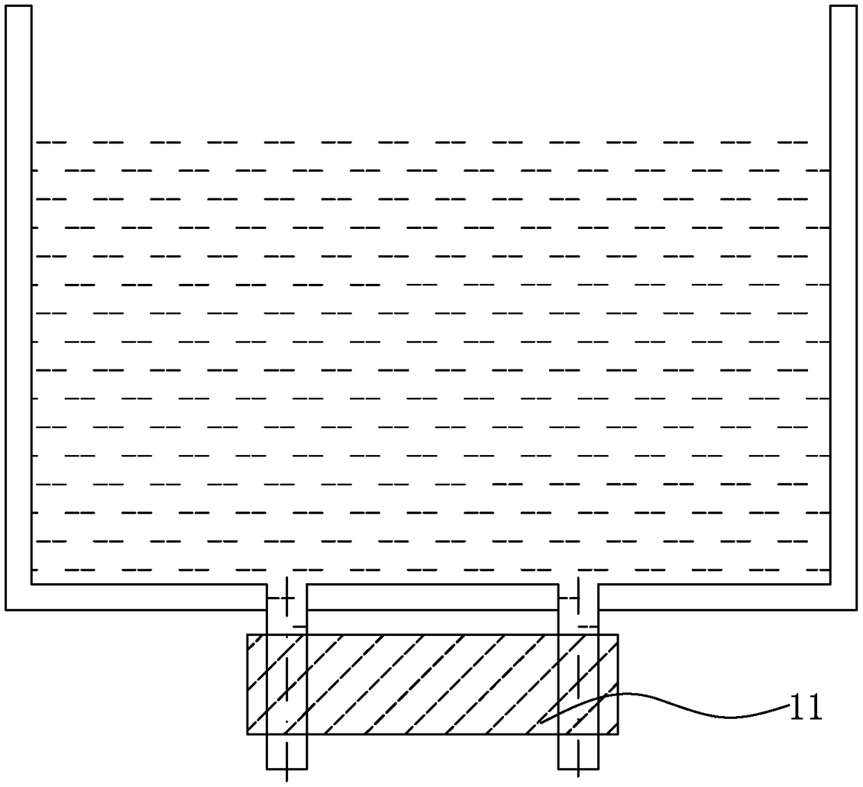
[0031] like Figure 1-7 In the specific embodiment shown, the preparation method of a phosphor copper anode for integrated circuits provided in this embodiment can be applied to the process of electroplating copper for integrated circuits, electroplating copper for high-end PCBs, and electroplating copper for high-end surface treatment, so that the manufacturing process is simple , the prepared phosphorus copper anode for integrated circuits has high filling capacity, and has higher ductility, high purity copper and small and uniform grain size.

[0032] like figure 1 Shown, a kind of preparation method of phosphor copper anode for integrated circuit comprises:

[0033] The raw materials are A-grade electrolytic copper with a coppe...


PUM

PropertyMeasurementUnit
thicknessaaaaaaaaaa
thicknessaaaaaaaaaa
thicknessaaaaaaaaaa

Abstract

The invention relates to a method, smelting furnace and system for preparing a phosphor-copper anode for an integrated circuit. The method comprises the steps that A-grade electrolytic copper with the copper content reaching 99.99% or above and a high-phosphor-copper alloy with the content of each single impurity not greater than 0.003% are adopted as raw materials; vacuum smelting and continuous casting are conducted, wherein the vacuum smelting furnace is selected for conducting copper-phosphor synthesis and traction on the A-grade electrolytic copper and the high-phosphor-copper alloy, so that a phosphor-copper alloy ingot is obtained; microcrystal treatment is conducted, wherein microcrystal treatment is conducted on the phosphor-copper alloy ingot in the vacuum state; and cold-state processing for formation is conducted, wherein processing for formation is conducted on the phosphor-copper alloy ingot obtained after microcrystal treatment at the normal temperature, so that the phosphor-copper anode for the integrated circuit is obtained. According to the method, smelting furnace and system for preparing the phosphor-copper anode for the integrated circuit, vacuum smelting and continuous casting are conducted on the raw materials; microcrystal treatment is conducted in the vacuum state; processing for formation is conducted at the normal temperature; the production process is simple; the prepared phosphor-copper anode for the integrated circuit has higher filling capacity and higher ductility; and copper is high in purity and small and uniform in grain size.

Description

technical field [0001] The invention relates to a preparation method of a phosphor copper anode, more specifically a preparation method of a phosphor copper anode for an integrated circuit and a system thereof. Background technique [0002] In the production of large-scale integrated circuits, copper etching is very difficult. It will become the future development direction of integrated circuits to prepare copper interconnection lines by electroplating copper process in production. Copper plating with a dense layer and uniform distribution, due to the fine grooves, requires the phosphor copper anode for electroplating to have a high filling capacity and higher ductility, and has higher requirements for the purity and grain size of copper , and, in integrated circuits, the oxygen content of copper plating is required to be high, because when the oxygen content is high, copper oxide and cuprous oxide are easily produced and distributed at the grain boundaries, affecting the p...

Claims


Application Information

Patent Timeline
Patent Type & Authority Patents(China)
IPC IPC(8): C22C1/03C22C9/00B22D11/14C22F1/08
CPCB22D11/004B22D11/14C22C1/03C22C9/00C22F1/08
Inventor 林伟文谭发棠周建新周腾芳
Owner 佛山市承安集团股份有限公司
Why Eureka
Try Eureka