Manufacturing method of drilled display panel and silk screen printing plate
A technology of screen printing screen and display panel, applied in nonlinear optics, instruments, optics, etc., can solve the problem of easy leakage of liquid crystal, rupture and separation of array substrate and color filter substrate, and inability to completely and reliably seal the sealant in the drilling area, etc. problems, to achieve the effect of eliminating easy leakage of liquid crystal and improving product quality and stability
- Summary
- Abstract
- Description
- Claims
- Application Information
AI Technical Summary
Problems solved by technology
Method used
Image
Examples
Embodiment 1
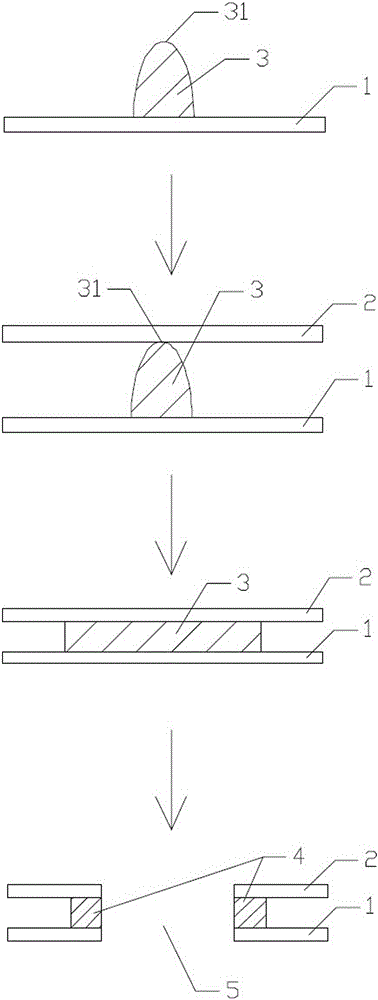
[0038] A method for manufacturing a drilled display panel, selecting the drilled hole diameter d of the drilled display panel 2 About 2.0mm, sealing ring width d 3 About 0.6mm, then the curing diameter d 1 About 3.5mm, the volume of the sealant in the drilling area (that is, the leakage volume of the sealant in the drilling area during silk screen printing) V is about π(3.5 / 2) 2 *h 1 ; the method includes the following steps:
[0039] An array substrate and a color filter substrate are provided; the array substrate has a drilling area, a display area, and a frame area, and the display area is between the drilling area and the frame area; the color filter substrate is connected to the array substrate Correspondingly, it also has a drilling area, a display area and a frame area, and the display area is between the drilling area and the frame area;
[0040] Provide the first screen printing screen and the second screen printing screen; the first screen printing screen adopts ...
Embodiment 2
[0046] A method for manufacturing a drilled display panel, selecting the drilled hole diameter d of the drilled display panel 2 About 2.0mm, sealing ring width d 3 About 0.6mm, then the curing diameter d 1 About 3.5mm, the volume of the sealant in the drilling area (that is, the leakage volume of the sealant in the drilling area during silk screen printing) V is about π(3.5 / 2) 2 *h 1 ; the method includes the following steps:
[0047] An array substrate and a color filter substrate are provided; the array substrate has a drilling area, a display area, and a frame area, and the display area is between the drilling area and the frame area; the color filter substrate is connected to the array substrate Correspondingly, there is a drilling area, a display area and a frame area on it, and the display area is between the drilling area and the frame area;
[0048] Provide the first screen printing screen and the second screen printing screen; the first screen printing screen adop...
Embodiment 3
[0054] A method for manufacturing a drilled display panel, selecting the drilled hole diameter d of the drilled display panel 2 About 2.0mm, sealing ring width d 3 About 0.6mm, then the curing diameter d 1 About 3.5mm, the volume of the sealant in the drilling area (that is, the leakage volume of the sealant in the drilling area during silk screen printing) V is about π(3.5 / 2) 2 *h1; the method includes the following steps:
[0055] An array substrate and a color filter substrate are provided; the array substrate has a drilling area, a display area, and a frame area, and the display area is between the drilling area and the frame area; the color filter substrate is connected to the array substrate Correspondingly, there is a drilling area, a display area and a frame area on it, and the display area is between the drilling area and the frame area;
[0056] Provide the first screen printing screen and the second screen printing screen; the first screen printing screen adopts ...
PUM
| Property | Measurement | Unit |
|---|---|---|
| thickness | aaaaa | aaaaa |
| thickness | aaaaa | aaaaa |
| thickness | aaaaa | aaaaa |
Abstract
Description
Claims
Application Information


