A kind of array substrate, display panel and display device

A technology for array substrates and pixel arrays, applied in instruments, semiconductor devices, optics, etc., can solve problems such as short circuit and disconnection of light-shielding layers, achieve the effects of reducing static electricity accumulation, avoiding disconnection, and solving short circuit problems

Active Publication Date: 2020-06-19
XIAMEN TIANMA MICRO ELECTRONICS +1
View PDF10 Cites 0 Cited by
  • Summary
  • Abstract
  • Description
  • Claims
  • Application Information

AI Technical Summary

Problems solved by technology

[0005] In view of this, the present invention provides an array substrate, a display panel and a display device to solve the pro

Method used


Image

  • A kind of array substrate, display panel and display device
  • A kind of array substrate, display panel and display device
  • A kind of array substrate, display panel and display device

Examples


Example Embodiment

[0041] The technical solutions in the embodiments of the present invention will be clearly and completely described below in conjunction with the accompanying drawings in the embodiments of the present invention. Obviously, the described embodiments are only a part of the embodiments of the present invention, rather than all the embodiments. Based on the embodiments of the present invention, all other embodiments obtained by those of ordinary skill in the art without creative work shall fall within the protection scope of the present invention.

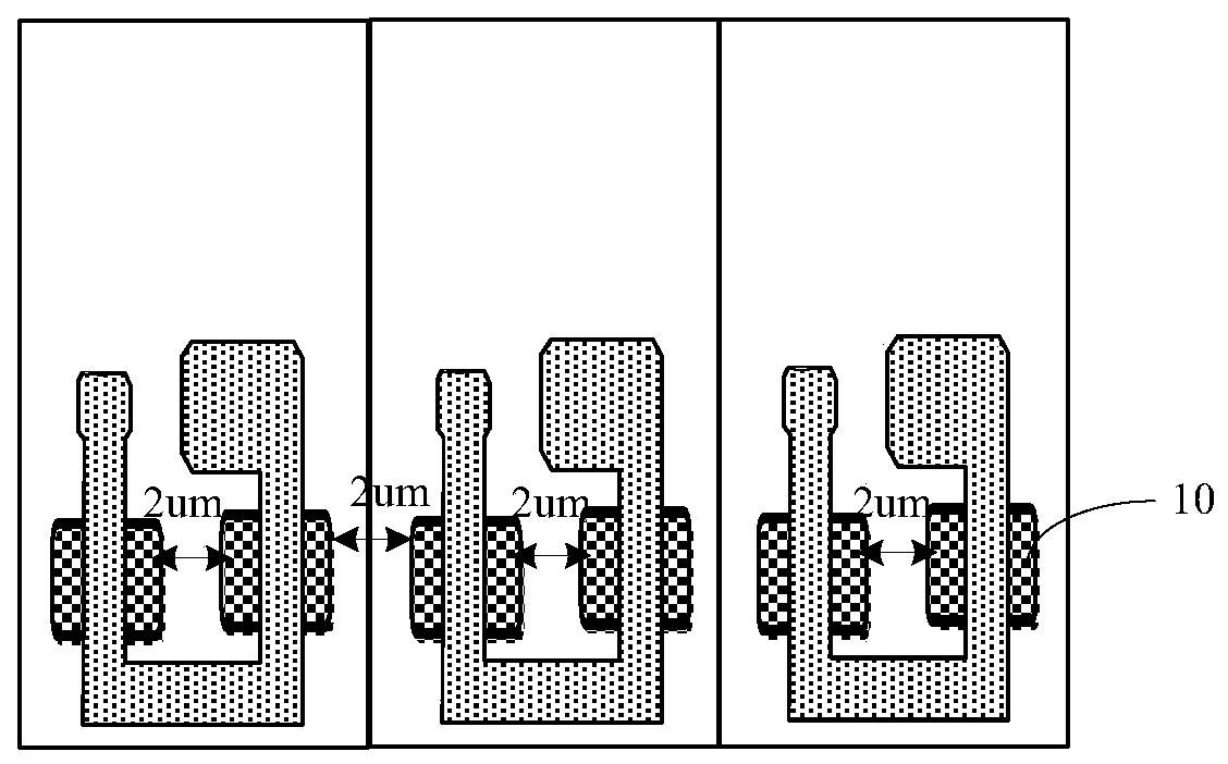
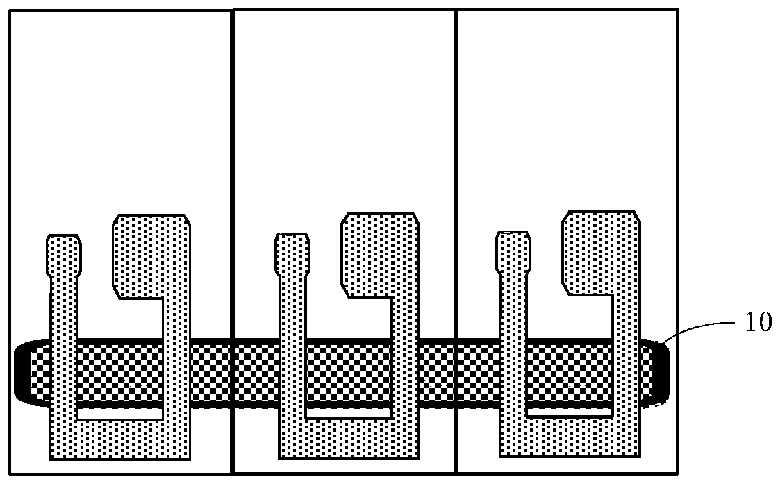
[0042] In the array substrate provided by the present invention, in the same row of the pixel array, the projections of the light shielding layers of at least two pixel subunits in the extending direction of the gate line are not completely overlapped, so that a certain adjacent pixel Staggered up and down. As the pixels are staggered up and down, the linear spacing between the corresponding light-shielding layers becomes larger, thereby...


PUM


Abstract

The invention provides an array substrate, a display panel and a display device. In the array substrate, in the same row of a pixel array, the projections of the shading layer of at least two pixel sub-units in the extension direction of a grid line are not completely overlapped so that adjacent pixels are staggered up and down. Since the pixels are staggered up and down, the linear space between corresponding shading layers is increased, and the problem of short circuit caused by a too small design clearance of the shading layers is solved. Moreover, since the pixels are staggered up and down, corresponding shading layers are not continuous, the length of a single shading layer is relatively short, then the static accumulation on the shading layer is reduced, and static injury happens less in comparison with a strip shading layer; and when one shading layer encounters static injury, the problem of broken line of the shading layers and the grid line is further avoided.

Description

Technical field [0001] The present invention relates to the field of liquid crystal display technology, and more specifically, to an array substrate, a display panel and a display device. Background technique [0002] With the continuous development of technology, users' requirements for the size and resolution of LCD screens have gradually increased. The pixel density PPI (Pixel Per Inch) of the liquid crystal display directly affects the resolution of the screen. As the pixel density of the liquid crystal display increases, the pixel pitch of the liquid crystal display is getting smaller and smaller. In addition, since a light shielding layer needs to be provided on the pixels, the design gap of the light shielding layer between the pixels becomes smaller and smaller. [0003] For example, when the pixel density of the LCD screen is 4K, please refer to figure 1 , The design gap of the light shielding layer 10 is usually 2um. Or like figure 2 As shown, the light shielding layer...

Claims


Application Information

Patent Timeline
IPC IPC(8): G02F1/1362G02F1/1368H01L27/12
CPCG02F1/136209G02F1/136286G02F1/1368G02F2202/22H01L27/1214
Inventor 陈彬彬
Owner XIAMEN TIANMA MICRO ELECTRONICS
Why Eureka
Try Eureka