Double-stage self-aligning contact window and manufacturing method thereof

A manufacturing method and contact window technology are applied in semiconductor/solid-state device manufacturing, electrical components, electrical solid-state devices, etc., to achieve the effects of increasing process space, increasing yield, and reducing the difficulty of etching

Active Publication Date: 2008-10-08
UNITED MICROELECTRONICS CORP
View PDF2 Cites 0 Cited by
  • Summary
  • Abstract
  • Description
  • Claims
  • Application Information

AI Technical Summary

Problems solved by technology

[0009] The invention provides an etching process for self-aligning contact windows, which can improve the alignment accuracy space (Aligned accu

Method used


Image

  • Double-stage self-aligning contact window and manufacturing method thereof
  • Double-stage self-aligning contact window and manufacturing method thereof
  • Double-stage self-aligning contact window and manufacturing method thereof

Examples


Example Embodiment

[0053] Example one

[0054] Figure 2A to Figure 2F It is a cross-sectional view of a manufacturing method of a semiconductor device according to an embodiment of the present invention.

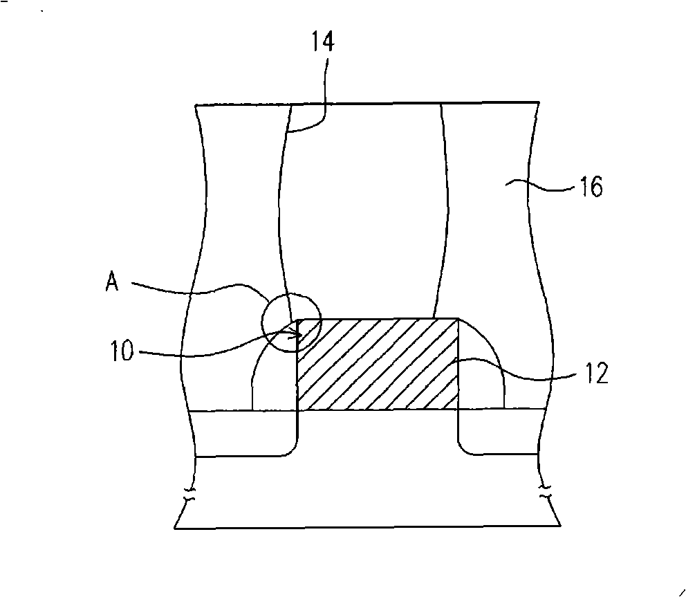
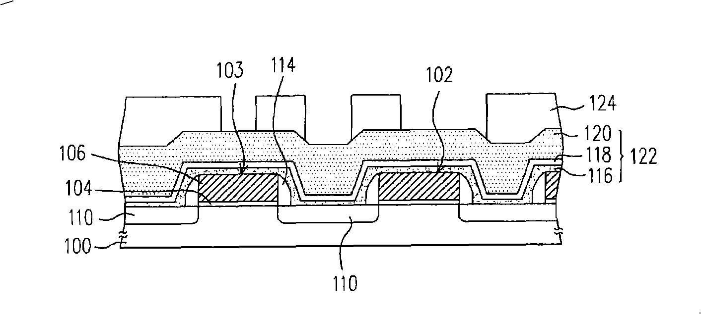
[0055] Please refer to Figure 2A , First provide the substrate 100. The substrate 100 is, for example, a silicon substrate, such as an N-type silicon substrate or a P-type silicon substrate. Of course, the substrate 100 may also be a substrate with silicon on an insulating layer or the like. Transistors 102 and 103 have been formed on the substrate 100. The transistors 102 and 103 are, for example, N-channel metal oxide semiconductor conductor elements (NMOS) or P-channel metal oxide semiconductor conductor elements (PMOS).

[0056] The transistors 102 and 103 may be composed of a gate dielectric layer 104, a gate 106, a spacer 114, and a source / drain region 110, respectively. The gate dielectric layer 104 is located between the gate 106 and the substrate 100. The material of the gate dielectri...

Example Embodiment

[0073] Example two

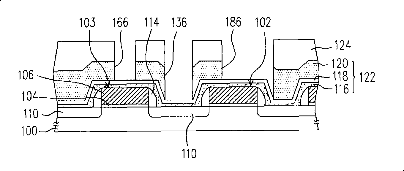
[0074] Figure 3A to 3H It is a flow cross-sectional view of another method for manufacturing a semiconductor device according to an embodiment of the present invention.

[0075] Please refer to Figure 3A versus 3BAccording to the method described in the embodiment, the dielectric layer 122 on the substrate 100 is subjected to a first-stage patterning process to form a lower opening 136 in the dielectric layer 122 corresponding to the source / drain regions 110, The lower opening 166 corresponding to the gate 106 of the transistor 103 and the lower opening 186 corresponding to the gate 106 of the transistor 102 and the source / drain region 110 of the transistor 103.

[0076] Please refer to Figure 3C After removing the photoresist layer 124, a conformal liner material layer 150 is first formed on the substrate 100 to cover the dielectric layer 122 and the sidewalls and bottoms of the lower openings 136, 166, and 186. The material of the liner material layer 15...


PUM


Abstract

A preparation method for double-stage automatic aligning contact window includes: forming a first dielectric layer on a substrate having a contact region; forming a bottom opening in the first dielectric layer corresponding to the contact region; forming a second dielectric layer on the first dielectric layer; forming a upper opening in the second dielectric layer, wherein the upper opening automatically aligns to the bottom opening and communicates with the bottom opening, thereby forming an automatic aligning contact window opening; and finally forming a conductive layer in the automatic aligning contact window opening.

Description

Technical field [0001] The invention relates to an integrated circuit element and a manufacturing method thereof, and more particularly to a two-stage self-aligned contact (SAC) and a manufacturing method thereof. Background technique [0002] With the advancement of science and technology, the manufacturing of electronic components must increase the degree of integration to meet the trend of light, thin, short, and small electronic components. In addition to reducing the size of the semiconductor element itself, the method of increasing the integration degree can also be achieved by reducing the distance between the semiconductor elements. However, no matter whether the size of the semiconductor device itself is reduced, or the distance between the semiconductor devices is reduced, some process problems will occur. [0003] Taking the process of self-aligning the contact window as an example, after the size of the contact window is reduced, its aspect ratio increases, the etchin...

Claims


Application Information

Patent Timeline
IPC IPC(8): H01L21/768H01L23/522
Inventor 周玲君陈铭聪曹博昭
Owner UNITED MICROELECTRONICS CORP
Why Eureka
Try Eureka