Preparation method of silicon oxide layer for solar cell and solar cell

A technology for solar cells and silicon oxide layers, applied in the field of solar cells, can solve the problems of low content of high-valence silicon, difficult to control thickness, small thickness of silicon oxide layer, etc. Effect

Active Publication Date: 2019-09-06
NINGBO INST OF MATERIALS TECH & ENG CHINESE ACADEMY OF SCI
View PDF3 Cites 0 Cited by
  • Summary
  • Abstract
  • Description
  • Claims
  • Application Information

AI Technical Summary

Problems solved by technology

[0007] Based on this, it is necessary to provide a method for preparing a silicon oxide layer of a solar cell and its preparation for the problems that the thickness and quality of the silicon oxide layer are not easy to control in the prior art, or the thickness of the prepared silicon oxide layer is small, and the content of high-valence silicon is low. silicon oxide layer and solar cells

Method used


Image

  • Preparation method of silicon oxide layer for solar cell and solar cell
  • Preparation method of silicon oxide layer for solar cell and solar cell
  • Preparation method of silicon oxide layer for solar cell and solar cell

Examples


Embodiment 1

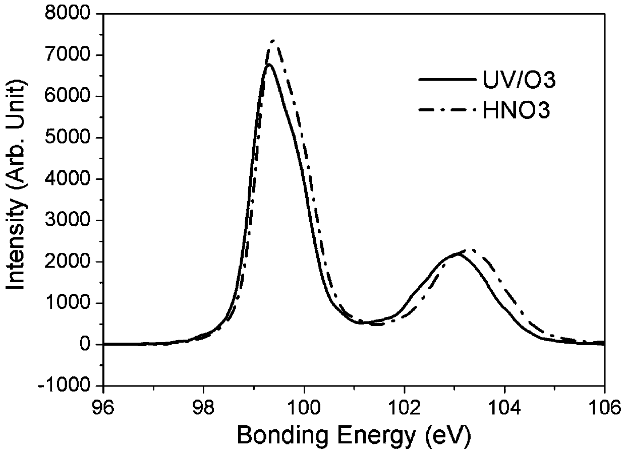
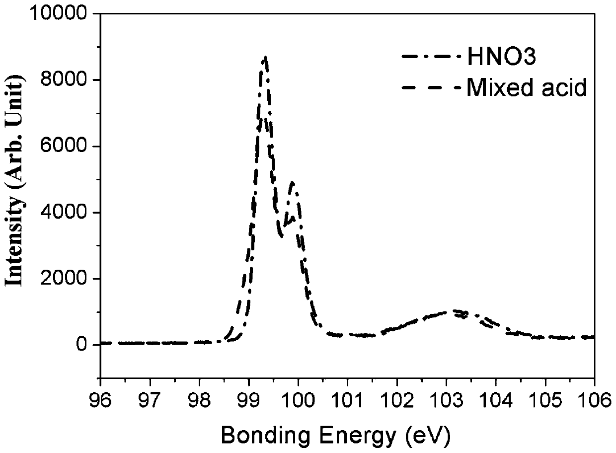
[0055] The oriented n-type silicon wafer is pretreated, that is, the silicon wafer is first cleaned by RCA standard cleaning method, and then the native oxide layer on the surface of the silicon wafer is removed by HF; the pretreated silicon wafer is placed in a temperature of 20°C Oxidation treatment for 2 minutes in the mixed acid solution, wherein the mixed acid solution is formed by mixing nitric acid (68%) and sulfuric acid (98%) at a volume ratio of 3:1.

[0056] The thickness of the silicon oxide layer was measured to be 1.2 nm by spectroscopic ellipsometry.

Embodiment 2

[0058] The oriented n-type silicon wafer is pretreated, that is, the silicon wafer is first cleaned by RCA standard cleaning method, and then the original oxide layer on the surface of the silicon wafer is removed by HF; the pretreated silicon wafer is placed in a temperature of 120 ° C Oxidation treatment in the mixed acid solution for 10 minutes, wherein the mixed acid solution is formed by mixing nitric acid (68%) and sulfuric acid (98%) at a volume ratio of 9:1.

[0059] The thickness of the silicon oxide layer was measured by spectroscopic ellipsometry to be 2.3 nm.

Embodiment 3

[0061] Pretreat the oriented n-type silicon wafer, that is, the silicon wafer is first cleaned by RCA standard cleaning method, and then the native oxide layer on the surface of the silicon wafer is removed by HF; the pretreated silicon wafer is placed in a temperature of 90 ° C Oxidation treatment in the mixed acid solution for 10 minutes, wherein the mixed acid solution is formed by mixing nitric acid (68%) and sulfuric acid (98%) at a volume ratio of 1:1.

[0062] The thickness of the silicon oxide layer was measured to be 2.0 nm by spectroscopic ellipsometry.


PUM


Abstract

The invention provides a method for preparing a silicon oxide layer. The preparation method includes the following steps: placing a silicon chip in a mixed acid solution for oxidation treatment, and the mixed acid solution is a mixed solution of nitric acid and sulfuric acid; wherein the nitric acid 1. The sulfuric acid mixture is formed by mixing 68% concentrated nitric acid and 98% concentrated nitric acid at a volume ratio of 1:1 to 10:1. The preparation method of the above-mentioned silicon oxide layer, 1) can achieve a more efficient oxidation effect on the silicon surface, the silicon in the silicon oxide layer is oxidized more thoroughly, and the proportion of silicon in a high-valence state increases; 2) the preparation temperature is low, and can be obtained at as low as A silicon oxide layer with a thickness greater than 1.4nm is prepared under the condition of 20°C, which meets the needs of preparing solar cells; 3) The processing time is shortened, for example, a silicon oxide layer with a thickness greater than 1.4nm can be prepared in 2 to 4 minutes; 4) The oxide layer The thickness is appropriate, the prepared silicon oxide layer can be controlled within 1.0-3.0 nm, and the thickness of the silicon oxide layer can completely cover the thickness requirement required by the device.

Description

technical field [0001] The invention relates to the field of solar cells, in particular to a method for preparing a silicon oxide layer of a solar cell and the solar cell. Background technique [0002] The Tunneling Oxide Passivation Contact (TOPCon) solar cell is a new type of silicon solar cell proposed by the Fraunhofer Institute in Germany in the past two years. The battery uses an n-type silicon wafer, and the back of the silicon wafer is covered with a silicon oxide layer with a thickness of less than 2nm, and then covered with a doped polysilicon or amorphous silicon layer. The back structure of the battery is n-type silicon wafer / ultra-thin silicon oxide layer / n+ polysilicon layer / metal electrode layer. When the battery is working, electrons tunnel from the n-type silicon slice through the silicon oxide layer through the silicon oxide into the doped polysilicon layer / amorphous silicon layer. The silicon oxide layer therein can have an excellent passivation effect o...

Claims


Application Information

Patent Timeline
Patent Type & Authority Patents(China)
IPC IPC(8): H01L31/18H01L31/042
CPCH01L31/042H01L31/1868Y02E10/50Y02P70/50
Inventor 叶继春曾俞衡高平奇童慧蔡亮廖明墩王丹
Owner NINGBO INST OF MATERIALS TECH & ENG CHINESE ACADEMY OF SCI
Why Eureka
Try Eureka