Encapsulating method of COB (chip-on-board) display module and display module

An encapsulation method and technology for display modules, which are used in identification devices, instruments, etc., can solve the problems of inability to completely avoid light mixing, ineffective absorption by light-shielding layers, uneven filling, etc., to avoid light mixing, reduce spacing, and reduce injection. effect of difficulty

Active Publication Date: 2017-03-08
FOSHAN NATIONSTAR OPTOELECTRONICS CO LTD
View PDF7 Cites 14 Cited by
  • Summary
  • Abstract
  • Description
  • Claims
  • Application Information

AI Technical Summary

Problems solved by technology

[0005] However, since the slit 16 is formed by molding, the depth of the slit 16 is less than the thickness of the protective layer 15, and the slit 16 does not touch the upper surface of the substrate 11, so that part of the light emitted by the adjacent light-emitting unit 13 will pass through the slit. The protective layer between the lower part of 16 and the upper surface of the substrate 11 produces mixed light, which cannot be completely avoided; and the bottom of the slit 16 is not connected to the air, and it is easy to cause filling when epoxy resin AB glue is filled in the slit Inhomogeneity or defects such as bubbles, the formed light-shielding layer cannot effectively absorb or reflect the light emitted by the light-emitting unit 13

Method used


Image

  • Encapsulating method of COB (chip-on-board) display module and display module
  • Encapsulating method of COB (chip-on-board) display module and display module
  • Encapsulating method of COB (chip-on-board) display module and display module

Examples


Embodiment 1

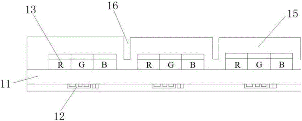
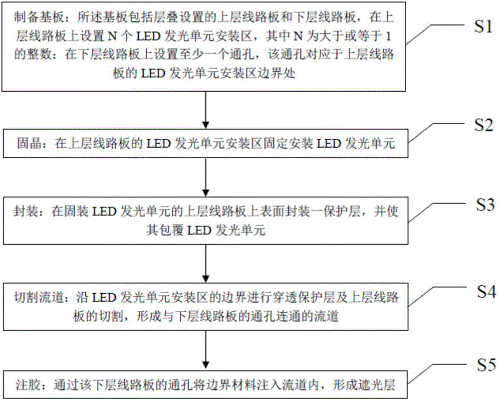
[0044] see figure 2 , which is a flow chart of the packaging method of the COB display module of the present invention, the packaging structure of the COB display module of the present invention can be realized through the following steps:

[0045] Step S1 : Prepare the substrate 100 .

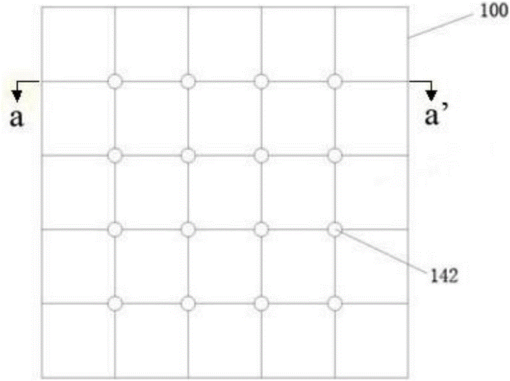
[0046] see image 3 with Figure 4 , which are respectively a bottom plan view and a cross-sectional view of the substrate 100 in step S1 of the present invention. In this embodiment, the substrate 100 includes an upper layer circuit board 120 and a lower layer circuit board 140 that are stacked. Both the upper layer circuit board 120 and the lower layer circuit board 140 may be single-layer circuit boards or multi-layer circuit boards. On the upper circuit board 120, N LED light-emitting unit installation areas 122 for arranging N groups of light-emitting units are arranged, wherein N is an integer greater than or equal to 1. The LED lighting unit installation area 122 set in this step i...

Embodiment 2

[0060] The content of this embodiment is basically the same as that of Embodiment 1, the difference lies in the step S5 of the encapsulation method of the COB display module and the structure of the COB display module.

[0061] In step S5, the boundary material is injected using a mold provided with grooves, and the substrate 100 is placed in the mold, wherein the bottom surface of the lower circuit board 140 is in contact with the grooves of the mold. In the injection process, the boundary material is injected from the mold, and a certain injection pressure is used to make the boundary material pass through the groove on the mold from the bottom of the lower circuit board 140, distribute into the through hole 142 and flow into the flow channel 124, and in the lower circuit board 140. The bottom surface of the plate 140 forms a balancing layer 500 corresponding to the shape of the mold groove. Through this injection method, the multi-channel injection of the boundary material ...

Embodiment 3

[0064] The content of this embodiment is basically the same as that of Embodiment 1, the difference lies in the steps S1 and S5 of the encapsulation method of the COB display module and the structure of the COB display module.

[0065] In step S1, a channel is further provided on the bottom surface of the lower circuit board 140 by means of a mold or cutting, and the channel communicates with the through hole on the lower circuit board at the same time, and its shape and depth can be adjusted according to the actual design. The shape of the channel is grid-like, and may also be dendrite-like or the like.

[0066] In step S5, the boundary material is injected into the channel, and the boundary material is distributed into the through hole through the channel, so as to form a balance layer embedded in the channel and the through hole on the bottom surface of the lower circuit board 140, through the The method obtained is a COB display module formed on both sides of the boundary ...


PUM


Abstract

The invention relates to an encapsulating method of a COB (chip-on-board) display module and the display module. The encapsulating method of the COB display module comprises the following steps: S1: manufacturing a substrate, wherein the substrate comprises an upper circuit board and a lower circuit board which are arranged in a superposed mode, N pieces of LED light emitting unit mounting areas are arranged on the upper circuit board, wherein N is an integer which is greater than or equal to 1, and at least one through hole, which runs through the lower circuit board, is formed in the lower circuit board; S2: fixedly mounting LED light emitting units in the LED light emitting unit mounting areas of the upper circuit board; S3: encapsulating a protective layer on the surface of the upper circuit board and covering the LED light emitting units with the protective layer; S4: conducting cutting along the boundaries of the LED light emitting unit mounting areas in a mode of penetrating the protective layer and the upper circuit board, so as to form runners; and S5: injecting a boundary material into the runners through the through hole in the lower circuit board, so that a light shield layer is formed. According to the encapsulating method provided by the invention, glue injection can be conducted easily, and by virtue of the formed light shield layer, a mutual light mixing phenomenon between the adjacent LED light emitting units can be completely blocked, so that a contrast ratio is improved.

Description

technical field [0001] The invention belongs to the field of manufacturing photoelectric devices, and in particular relates to a packaging method of a COB display module and a display module thereof. Background technique [0002] In recent years, LED display technology has developed rapidly and is favored by people. It is widely used in large squares, financial markets, airports, banks, hospitals and shopping malls. With the development of LED display technology, products are increasingly developing in the direction of high-density, small-pitch and full-color high-resolution. At present, the minimum size range of RGB display discrete devices is 0.5-1.0mm. The miniaturization of a single device faces many problems such as chip assembly, packaging and testing, and the miniaturization manufacturing cost of RGB display discrete devices is relatively high. In addition, when discrete devices are used for display integration, the integration density of the display is reduced due t...

Claims


Application Information

Patent Timeline
Patent Type & Authority Applications(China)
IPC IPC(8): G09F9/33
Inventor 李宗涛李家声李宏浩吴灿标
Owner FOSHAN NATIONSTAR OPTOELECTRONICS CO LTD
Why Eureka
Try Eureka