

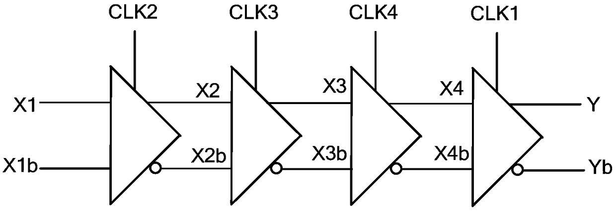
A controllable diode bootstrap adiabatic circuit and four-stage inverter/buffer
An adiabatic circuit and diode technology, applied in logic circuits, pulse technology, electrical components, etc., can solve the problems of increasing circuit instability, large delay, and large non-adiabatic power consumption, and achieve lower power consumption and lower delay. , the effect of simple circuit structure
- Summary
- Abstract
- Description
- Claims
- Application Information
AI Technical Summary
Problems solved by technology
Method used
Image

Examples
Embodiment 1
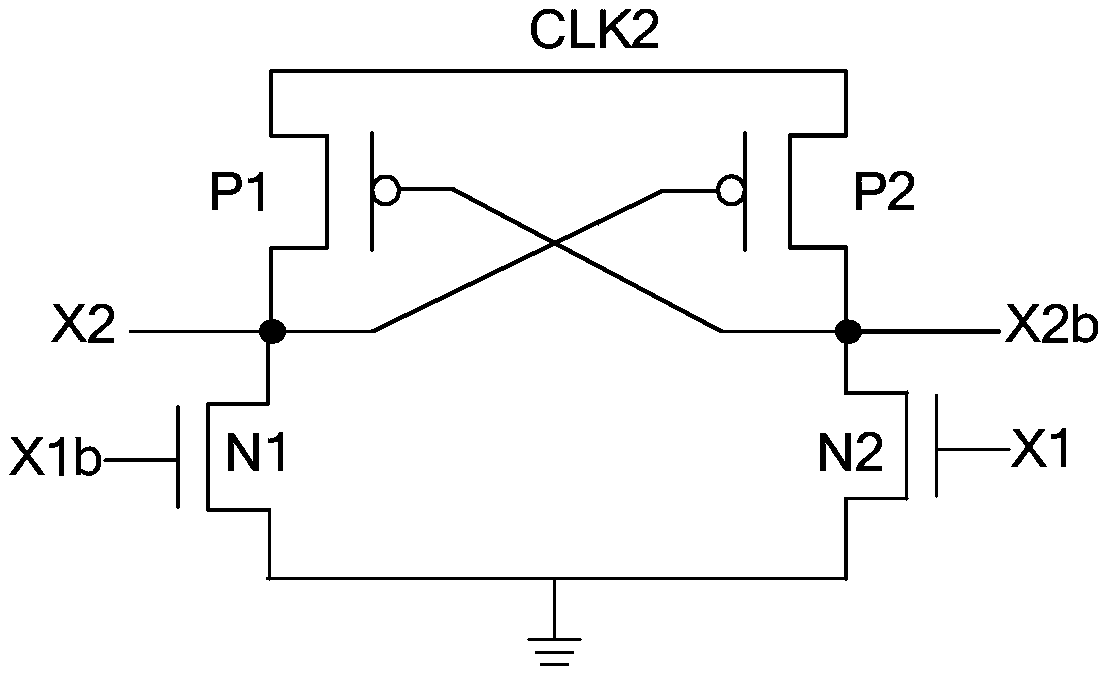
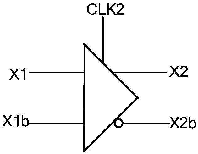
[0022] Embodiment 1: As shown in Figure 4(a) and Figure 4(b), a controllable diode bootstrap adiabatic circuit includes a first PMOS transistor P1, a second PMOS transistor P2, a first NMOS transistor N1, a second NMOS transistor N2, third NMOS transistor N3, fourth NMOS transistor N4, fifth NMOS transistor N5 and sixth NMOS transistor N6; the source of the first PMOS transistor P1, the source of the second PMOS transistor P2, the third NMOS transistor The drain of N3, the drain of the fourth NMOS transistor N4, the drain of the fifth NMOS transistor N5 and the drain of the sixth NMOS transistor N6 are connected, and the connection end is the clock end of the controllable diode bootstrap adiabatic circuit; the first The gate of the PMOS transistor P1, the drain of the second PMOS transistor P2, the source of the fourth NMOS transistor N4, the drain of the second NMOS transistor N2 and the gate of the sixth NMOS transistor N6 are connected, and the connection terminal is control...
Embodiment 2
[0023] Embodiment 2: As shown in Figure 4(a) and Figure 4(b), a controllable diode bootstrap adiabatic circuit includes a first PMOS transistor P1, a second PMOS transistor P2, a first NMOS transistor N1, a second NMOS transistor N2, third NMOS transistor N3, fourth NMOS transistor N4, fifth NMOS transistor N5 and sixth NMOS transistor N6; the source of the first PMOS transistor P1, the source of the second PMOS transistor P2, the third NMOS transistor The drain of N3, the drain of the fourth NMOS transistor N4, the drain of the fifth NMOS transistor N5 and the drain of the sixth NMOS transistor N6 are connected, and the connection end is the clock end of the controllable diode bootstrap adiabatic circuit; the first The gate of the PMOS transistor P1, the drain of the second PMOS transistor P2, the source of the fourth NMOS transistor N4, the drain of the second NMOS transistor N2 and the gate of the sixth NMOS transistor N6 are connected, and the connection terminal is control...
PUM
 Abstract
Description
Claims
Application Information