Unlock instant, AI-driven research and patent intelligence for your innovation.

A kind of thin film transistor array substrate and liquid crystal panel

A technology of thin film transistors and array substrates, which is applied in the field of voltage output control circuits and liquid crystal displays, can solve problems such as increasing power consumption of display modules, affecting display quality, and controlling signal glitches, so as to improve display quality, reduce power consumption, and avoid noise effect

Active Publication Date: 2019-12-03
WUHAN CHINA STAR OPTOELECTRONICS TECH CO LTD
View PDF5 Cites 0 Cited by
  • Summary
  • Abstract
  • Description
  • Claims
  • Application Information

AI Technical Summary

Problems solved by technology

But when all the multiplexers are turned on, it will cause the display module to instantly form a large pumping load on the LCD panel driver chip, which will cause glitches in the control signal output by the driver chip, which will not only affect the display quality, Noise is generated, and it will also increase the power consumption of the display module

Method used


Image

  • A kind of thin film transistor array substrate and liquid crystal panel
  • A kind of thin film transistor array substrate and liquid crystal panel
  • A kind of thin film transistor array substrate and liquid crystal panel

Examples


Embodiment Construction

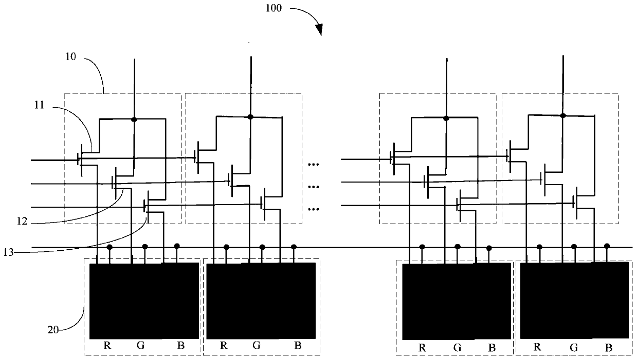
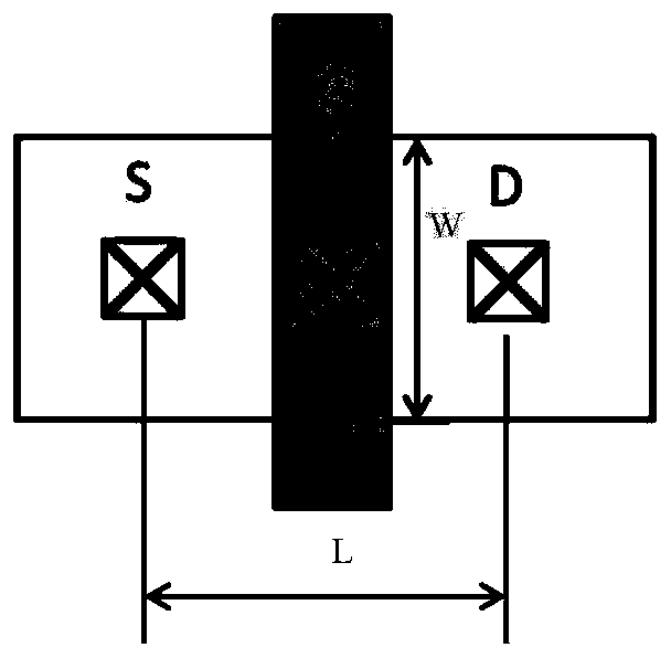
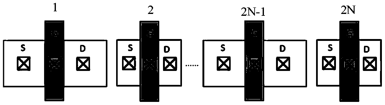
[0023] The following will clearly and completely describe the technical solutions in the embodiments of the present invention with reference to the accompanying drawings in the embodiments of the present invention. Obviously, the described embodiments are only part of the embodiments of the present invention, not all of them. Based on the embodiments of the present invention, all other embodiments obtained by persons of ordinary skill in the art without making creative efforts belong to the protection scope of the present invention.

[0024] In addition, the following descriptions of the various embodiments refer to the attached drawings to illustrate specific embodiments in which the present invention can be implemented. The directional terms mentioned in the present invention, for example, "upper", "lower", "front", "rear", "left", "right", "inner", "outer", "side", etc., only is to refer to the direction of the attached drawings. Therefore, the direction terms used are for ...


PUM


Abstract

The invention provides a thin film transistor array substrate which comprises sets of thin film transistors and a number of RGB pixel units. Each set of thin film transistor comprises three thin film transistors located in first, second and third rows. Three thin film transistors are corresponding to an R subpixel, a G subpixel and a B subpixel in a corresponding RGB pixel unit. The length-width ratio of conductive channels of all thin film transistors in each row is not exactly the same, but is within a preset ratio range, so that the total leakage current of the row is within a preset current range. The leakage current is only related to the width-length ratio of the conductive channel of the thin film transistor. The larger the width-length ratio W / L is, the larger the drain current is. The smaller the width-length ratio is, the smaller the drain current is. According to the invention, burrs in a control signal output by a driving chip are avoided; the display quality of a liquid crystal panel is improved; noise can be avoided; and the power consumption of a display module is reduced. The invention further provides the liquid crystal panel.

Description

technical field [0001] The invention relates to the field of display technology, in particular to a voltage output control circuit and a liquid crystal display. Background technique [0002] With the rapid development of the small and medium-sized electronic display industry, people have higher and higher requirements for the resolution and other quality of small and medium-sized LCD liquid crystal displays. The improvement of the display quality is closely related to the transmission rate of the display data and the integrity of the signal. For the current small and medium-sized LCD display screens, all the multiplexers are simultaneously turned on during the time period when the gates are turned on, so as to complete the charging of the RGB sub-pixels. But when all the multiplexers are turned on, it will cause the display module to instantly form a large pumping load on the LCD panel driver chip, which will cause glitches in the control signal output by the driver chip, w...

Claims


Application Information

Patent Timeline
Patent Type & Authority Patents(China)
IPC IPC(8): H01L27/12H01L29/10G02F1/1362G02F1/1368
CPCG02F1/13624G02F1/1368H01L27/1222H01L29/1033
Inventor 李曼黄俊宏左清成
Owner WUHAN CHINA STAR OPTOELECTRONICS TECH CO LTD