LED packaging structure

A technology of LED packaging and LED chips, which is applied in the direction of electrical components, circuits, semiconductor devices, etc., can solve the problems of poor color temperature uniformity, uncomfortable color temperature uniformity, hindering LED applications, etc., to increase light output rate and improve uniformity Effect

Pending Publication Date: 2017-03-22
CHINA JILIANG UNIV
View PDF0 Cites 0 Cited by
  • Summary
  • Abstract
  • Description
  • Claims
  • Application Information

AI Technical Summary

Problems solved by technology

Due to the small contact angle between the phosphor glue and the substrate, the phosphor layer is thick in the middle and thin at the edge, and this structure makes the unif

Method used


Image

  • LED packaging structure
  • LED packaging structure

Examples


Example Embodiment

[0015] Example one

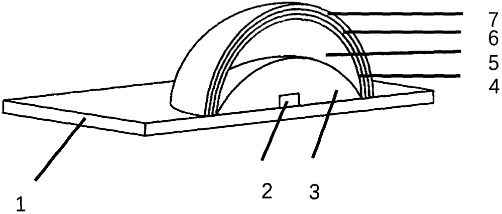
[0016] Such as figure 1 As shown, an LED packaging structure includes a substrate 1, an LED chip arranged on the substrate 1, a filling gel 3 for sealing the LED chip 2, a phosphor layer 6, a first gel layer 4, and a second gel Layer 7; the first colloid layer 4 is wrapped around the filling colloid 3 and forms a cavity 5 between the filling colloid 3; the middle of the cavity 5 is thick and the edges are thin; the phosphor layer 6 is coated on the first colloidal layer 4; the second colloidal layer 7 is coated on the phosphor layer 6.

Example Embodiment

[0017] Example two

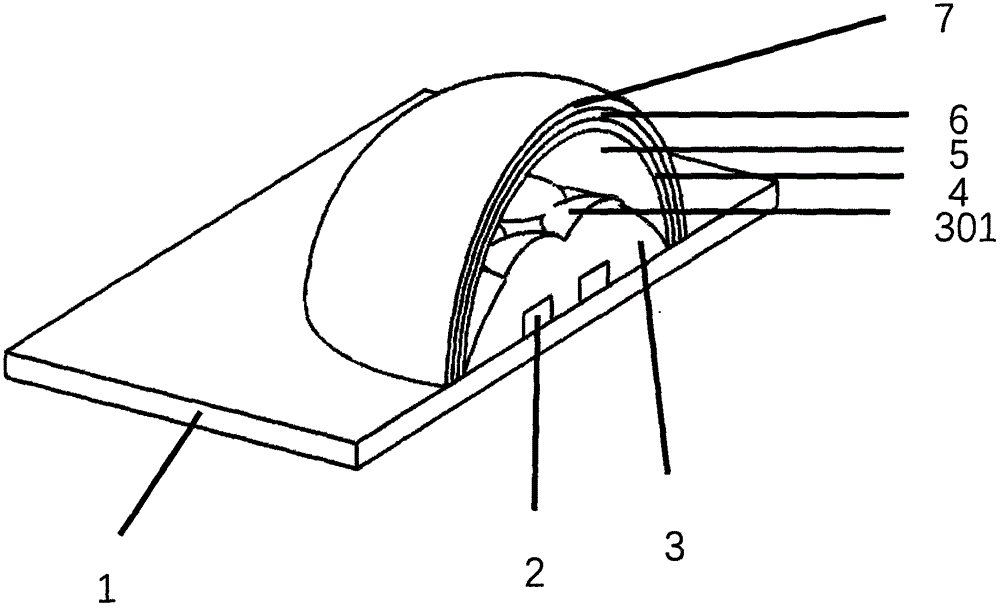
[0018] Such as figure 2 As shown, an LED packaging structure includes a substrate 1, an LED chip arranged on the substrate 1, a filling gel 3 for sealing the LED chip 2, a phosphor layer 6, a first gel layer 4, and a second gel Layer 7; the first colloid layer 4 is wrapped around the filling colloid 3, and forms a cavity 5 between the filling colloid 3; the phosphor layer 6 is wrapped in the first colloid layer 4 On; The second colloidal layer 7 is coated on the phosphor layer 6. The number of the LED chips 2 is greater than one, the surface of the filled colloid 3 has protrusions 301, and each protrusion 301 corresponds to one LED chip 2.

[0019] The light emitted by the LED chip 2 enters the filling colloid 3 and is refracted at the interface between the filling colloid 3 and the cavity 5. The blue light intensity is redistributed and reaches the phosphor layer 6 through the first colloid layer 4. Part of the blue light passes through the phosphor layer ...


PUM


Abstract

The invention discloses an LED packaging structure. The LED packaging structure comprises a substrate, LED chips arranged on the substrate, filling colloid for sealing the LED chips, a fluorescent powder layer, a first colloid layer and a second colloid layer, wherein the exterior of the filling colloid is coated with the first colloid layer, and a hollow cavity is formed between the filling colloid and the first colloid layer; the hollow cavity is thick in the middle and thin on the edge; the first colloid layer is coated with the fluorescent powder layer; and the fluorescent powder layer is coated with the second colloid layer. The LED packaging structure is simple in structure, easy to manufacture and capable of improving uniformity of color temperature.

Description

technical field [0001] The invention relates to the field of solid-state lighting, in particular to an LED packaging structure. Background technique [0002] LED is a solid-state semiconductor device. Compared with traditional incandescent lamps and fluorescent lamps, white LEDs have the advantages of low power consumption, high luminous efficiency, long service life, energy saving and environmental protection, and are widely used in street lighting, indoor lighting, Projector lighting and other fields. [0003] In order to realize a white light LED, the most common method is to coat a yellow phosphor powder on a blue light LED chip, and the blue light emitted by the chip and the yellow light emitted by the phosphor powder are mixed to form white light. Usually, phosphor and silica gel are mixed together to form phosphor glue, which is dropped directly on the LED chip. Due to the small contact angle between the phosphor glue and the substrate, the phosphor layer is thick i...

Claims


Application Information

Patent Timeline
IPC IPC(8): H01L33/58H01L33/54
CPCH01L33/58H01L33/54
Inventor 曹艳亭梁培舒海波黄杰郝锦玲杨晨
Owner CHINA JILIANG UNIV
Why Eureka
Try Eureka