Manipulator self provided with wafer edge-searching sensor

A sensor and manipulator technology, applied in the field of manipulators, can solve the problems of increased chip manufacturing costs, secondary contamination of wafers, and increased EFEM costs, and achieve the effect of continuous working, avoiding scratches and damage, and reducing secondary pollution.

Active Publication Date: 2017-04-05
芯导精密(北京)设备有限公司
View PDF5 Cites 16 Cited by
  • Summary
  • Abstract
  • Description
  • Claims
  • Application Information

AI Technical Summary

Problems solved by technology

[0006] The existing technology of the wafer transfer manipulator has technical defects in the following aspects: (1) The existing edge-seeking mechanism is that the tray rotates at high speed with the wafer, and the sensor for detecting the gap and the special camera do not rotate. It is easy to cause vibration and displacement of the high-speed rotating wafer, which can easily cause nano-scale particles and scratches on the back of the wafer and damage to the characteristics of the wafer chip, and these tiny damages will cause the rate of defective products in the wafer manufacturing process The catastrophic rise, especially in the current period of rapid development of the chip industry, the current feature size of the wafer circuit has reached 19 nanometers, and the thickness of the wafer is also continuously decreasing. Any tiny vibration will produce nano-scale particles, so that Wafers cause secondary pollution; cause irreparable losses (2) The transfer time of wafers in the prior art is long, and the manipulator needs to be taken out of the cassette and placed on the edge-finding mechanism fixed on the side of the cabinet, waiting for the mechanism After edge finding, camera OCR, and repositioning are completed, the manipulator retrieves the wafer and continues to transfer it to the designated position, which prolongs the overall wafer transfer time, which will reduce chip production efficiency and increase chip manufacturing costs; (3) Semiconductor 12 Almost every process in the chip manufacturing industry is inseparable from the transfer of the manipulator, and the manipulator manufacturers provide multiple functions in one package (EFEM). One set (sometimes two sets) of independent edge-finding mechanisms greatly increases the overall system EFEM cost
However, this invention has the following technical defects: the invention can only move horizontally in a fixed plane with the traditional edge-seeking mechanism in the X direction and cannot be raised and lowered with the main arm. Unable to truly realize the combination of edge finding and camera (OCR) work and manipulator

Method used


Image

  • Manipulator self provided with wafer edge-searching sensor
  • Manipulator self provided with wafer edge-searching sensor
  • Manipulator self provided with wafer edge-searching sensor

Examples


Embodiment 1

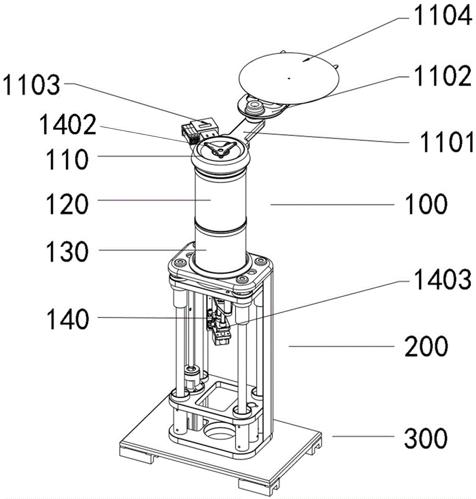
[0044] Such as figure 1 , 9 As shown, a manipulator equipped with a wafer edge detection sensor includes a main arm 100 , a mandrel assembly 140 , a manipulator lifting mechanism 200 and a slide 300 . The main arm 100 is located at the top and adopts a first hollow structure. Its lower end is fixedly connected to the manipulator lifting mechanism 200. The manipulator lifting mechanism 200 is fixedly connected to the sliding seat 300. The mandrel assembly 140 runs through the first hollow structure and is connected with the manipulator. The lifting mechanism 200 is connected.

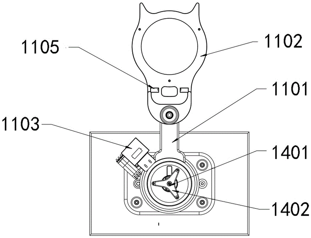
[0045] Such as figure 1 As shown, the main arm 100 includes a first main arm assembly 110 , a second main arm assembly 120 and a third main arm assembly 130 . The first main arm assembly 110 is located at the top, the bottom end of the first main arm assembly 110 is connected to the top end of the second main arm assembly 120, the bottom end of the second main arm assembly 120 is connected to the top ...

Embodiment 2

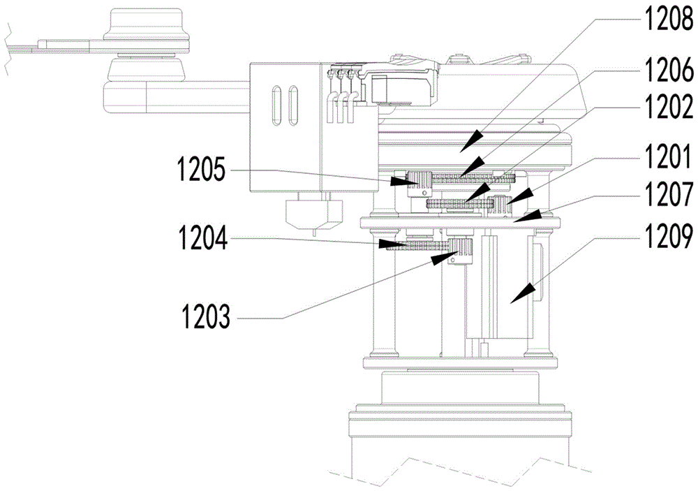
[0060] A manipulator with a built-in wafer edge detection sensor is similar to Embodiment 1, the difference is that it also includes a counterweight spring 206 and a lift limit mechanism.

[0061] Such as Figure 12 , as shown in 13, the lift limit mechanism includes a main arm limit piece 402 and a limit post 401. The main arm limiting piece 402 is disposed at the lower end of the main arm 100 and can rotate with the main arm 100 . The limit column 401 is located on the manipulator lifting mechanism 200 . Limit post limit piece 403 is arranged on limit post 401, and limit post limit piece 403 can be a plurality of annular pieces that are arranged at intervals, and the distance between adjacent limit post limit pieces 403 is the same as that in the cassette. Neighboring wafers are equally spaced.

[0062] Such as Figure 14 , as shown in 15, all the limiting posts 403 on the limiting post 401 and the limiting posts 401 together constitute the first electrode 4031, and the ...


PUM


Abstract

The invention relates to a manipulator self provided with a wafer edge-searching sensor, which comprises a main arm (100), an edge-searching sensor (1103) and a mandrel assembly (140), wherein the edge-searching sensor (1103) can lift and rotate along with the main arm (100); the main arm (100) adopts a first hollow structure; the mandrel assembly (140) passes through the first hollow structure and is arranged in a state of not rotating relative to the main arm (100) but lifting relative to the main arm (100); the mandrel assembly (140) adopts a hollow shaft to form a second hollow structure, the second hollow structure keeps an extraction state constantly, a tray (1402) supports the back part of the wafer, certain space is kept between the tray and the wafer, the certain space is communicated with the air to generate negative pressure, and thus, the tray (1402) can stabilize and support the wafer when the wafer is taken and fed. The edge-searching sensor and the manipulator are combined into one, the wafer does not rotate and the main arm drives the sensor to rotate at a high speed during the edge searching process, defects brought by rotating the wafer currently can be effectively avoided, and due to the negative pressure structure of the tray supporting the wafer, defects of the existing sucker structure can be overcome effectively.

Description

[0001] priority statement [0002] This application claims priority based on No. 201610349537.8 filed on May 24, 2016. All content of this application is incorporated by reference in this specification. technical field [0003] The invention relates to a manipulator for taking and delivering wafers, in particular to a wafer manipulator with a wafer edge detection sensor. Background technique [0004] At present, most of the wafer transfer manipulators are separated from the wafer edge detection mechanism, and a few of them move in the horizontal direction with the wafer edge detection mechanism, such as the edge detection sensor in the four-box (loadport) Sorter produced by Japan RORZE company. Aligner (x2) is to fix the edge finding mechanism on both sides of the device. [0005] The working procedure of the existing wafer transfer manipulator is: first take out the wafer from the wafer cassette and transfer it to the tray of the wafer edge-seeking mechanism, start the ce...

Claims


Application Information

Patent Timeline
Patent Type & Authority Applications(China)
IPC IPC(8): H01L21/687H01L21/683B25J9/08B25J15/06
Inventor 陈百捷王镇清姚广军
Owner 芯导精密(北京)设备有限公司
Why Eureka
Try Eureka