
Patsnap Eureka
For R&D, Patsnap Eureka makes reading and utilizing patents & technical documents easy.
Patsnap Eureka AIR
Designed for self-driven R&D workflows. Generate viable solutions, solve complex R&D challenges, empower your innovation with AI.

Patsnap Eureka Materials
Designed for material experts only. Revolutionize your material R&D, from search, analyze, to developing new materials.

TechResearch
Generate reliable direction feasibility study reports for your R&D in just a few steps.

TechSeek
Discover and master advanced knowledge NOW. Basics, ideas, possibilities, all at once.

TechMind
As an expert in R&D Theories, TechMind can generates customized viable solutions instantly.

TechRisk
Analyze your overall solution with one click, know your potential R&D risks in advance.

TechMonitor
Get weekly tech updates, stay abreast of the latest tech innovations and key insights.
Printed wiring board
A printed wiring board and wiring technology, applied in the directions of printed circuit, printed circuit, printed circuit manufacturing, etc., can solve the problems of difficult to form shielding, high shielding structure, etc., and achieve the effect of high shielding
- Summary
- Abstract
- Description
- Claims
- Application Information
AI Technical Summary
Problems solved by technology
Method used
Image

Examples
Embodiment 1
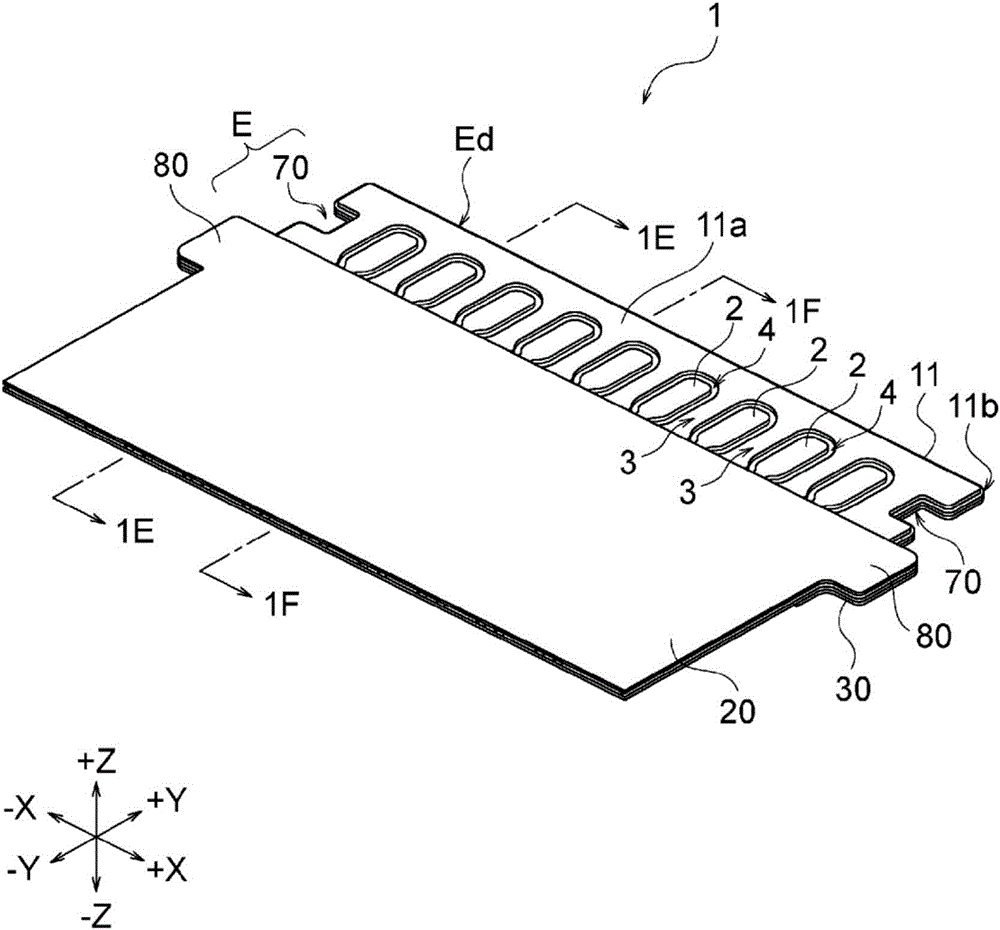
[0258] As Example 1, the model 1 of the printed wiring board 1 of the said 2nd example was defined. The model 1 of the printed wiring board 1 of the second example has Figure 2A ~ Figure 2Fconstruction shown. Moreover, in order to compare with Example 1, the model 1-2 of the printed wiring board which concerns on the comparative example 1 was defined. Model 1-2 of Comparative Example 1 was defined under the same conditions as Model 1 of Example 1 except for not having the groove 4 surrounding the pads 2a and 2b.
[0259] Such as Figure 9A As shown, the ground layer 3 is formed around the lands 2 a and 2 b of the model 1 of the printed wiring board 1 according to the first embodiment, and the groove 4 is formed between the lands 2 a and 2 b and the ground layer 3 . On the other hand, in the printed wiring board model 1-2 according to Comparative Example 1, no ground layer was formed around the pads (members corresponding to the pads 2a and 2b of this embodiment, the same b...
Embodiment 2
[0262] As Example 2, the model 2 of the structure which formed the ground layer 3 in the other main surface of the printed wiring board 1 of the said 2nd example was defined. The number of layers of the conductive layer of the printed wiring board of the model 2 of Example 2 was two layers. A ground layer is formed on one of the other main surfaces of the insulating base material. Moreover, in order to compare with this Example 2, the model 2-2 of the printed wiring board which concerns on the comparative example 2 was defined. Model 2-2 of Comparative Example 2 was tested under the same conditions as Model 2-1 of Example 2, except that the ground layer surrounding the entire circumference of the pad was not formed on one main surface of the insulating base material. defined.
[0263] Such as Figure 9A As shown, the model 2 of the printed wiring board 1 according to Example 2 has the groove 4, but the printed wiring board according to the model 2-2 of the comparative examp...
Embodiment 3
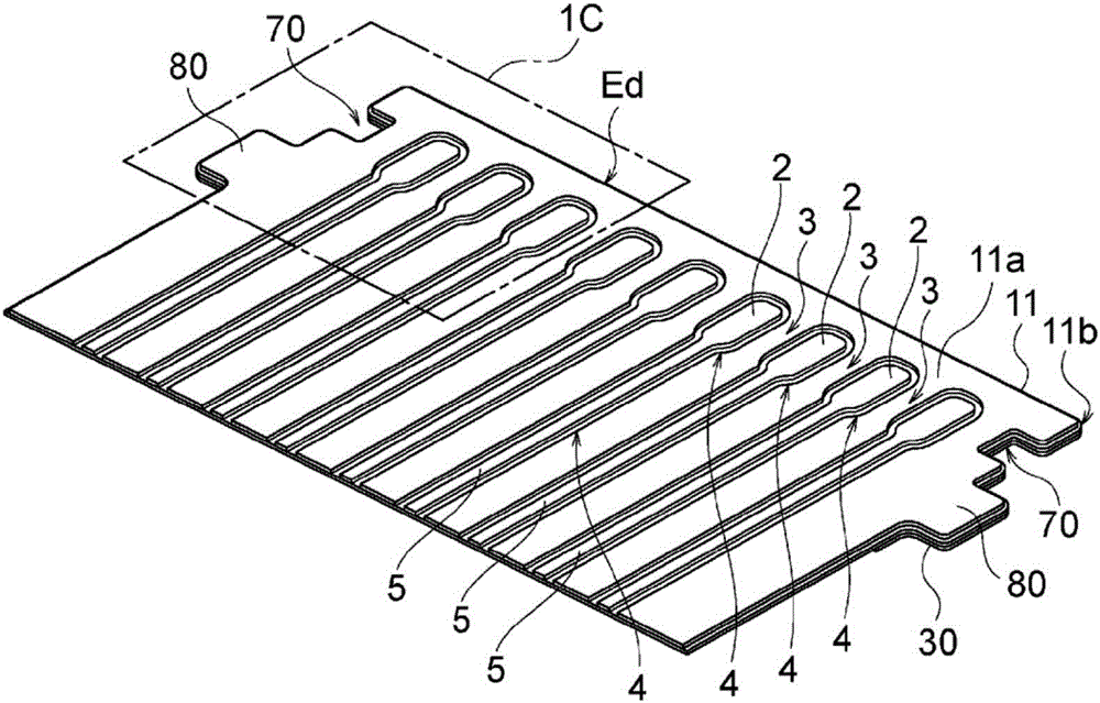
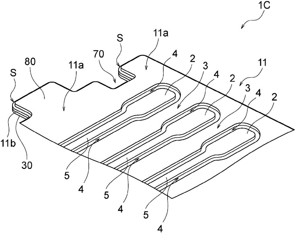
[0266] As Example 3, the model 3 of the printed wiring board 1 of the above-mentioned eighth example is defined. The number of layers of the conductive layer of the printed wiring board of model 2 was three layers. On one main surface of the insulating base material, a ground layer is not provided at a position closer to the connection end E side than the pad, and a ground layer is provided only on the side opposite to the connection end E. The model 3 of the printed wiring board 1 of the eighth example has Figure 8A ~ Figure 8H construction shown. Moreover, in order to compare with the model 3 of this Example 3, the model 3-2 of the printed wiring board which concerns on the comparative example 3 was defined. Model 3-2 of Comparative Example 3 was defined under the same conditions as Model 3 of Example 3 except that it did not have groove 4 surrounding pads 2a and 2b.
[0267] Such as Figure 9B As shown, the mold 3 of the printed wiring board 1 according to Example 3 ha...
PUM
 Abstract
Description
Claims
Application Information
 - R&D Engineer
- R&D Manager
- IP Professional
- Industry Leading Data Capabilities
- Powerful AI technology
- Patent DNA Extraction
Browse by: Latest US Patents, China's latest patents, Technical Efficacy Thesaurus, Application Domain, Technology Topic, Popular Technical Reports.
© 2024 PatSnap. All rights reserved.Legal|Privacy policy|Modern Slavery Act Transparency Statement|Sitemap|About US| Contact US: help@patsnap.com