

Wafer test system
A technology for wafer testing and testing values, applied in electronic circuit testing, electrical measurement, and measuring devices, etc., can solve problems such as inability to easily obtain wafer testing and testing information, and achieve the effect of improving data analysis efficiency
- Summary
- Abstract
- Description
- Claims
- Application Information
AI Technical Summary
Problems solved by technology
Method used
Image

Examples
Embodiment 1
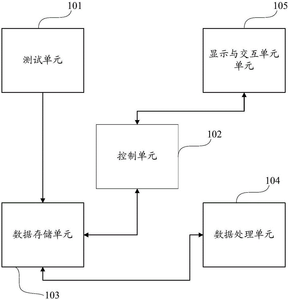
[0027] The invention provides a wafer test system, such as figure 1 As shown, it includes a test unit 101, a control unit 102, a data storage unit 103 and a display and interaction unit 105; the test unit 101 is used to test the wafer and store test data in the data storage unit 103; The control unit 102 extracts the test data of the specified test wafer from the data storage unit 103 according to the instruction received by the display and interaction unit 105, and controls the display and interaction unit 105 to display the specified test wafer through a two-dimensional image according to the specified display mode. Test wafer specific test data.
[0028] The wafer testing system of this embodiment further includes a data processing unit 104 , the data processing unit 104 organizes the test data in the data storage unit 103 , and stores the sorted test data in the data storage unit 103 . Specifically, the sorted test data includes the following information: test item type, ...
Embodiment 2
[0033] The difference between this embodiment and the first embodiment lies in that the display modes of the display and interaction unit 105 are different.
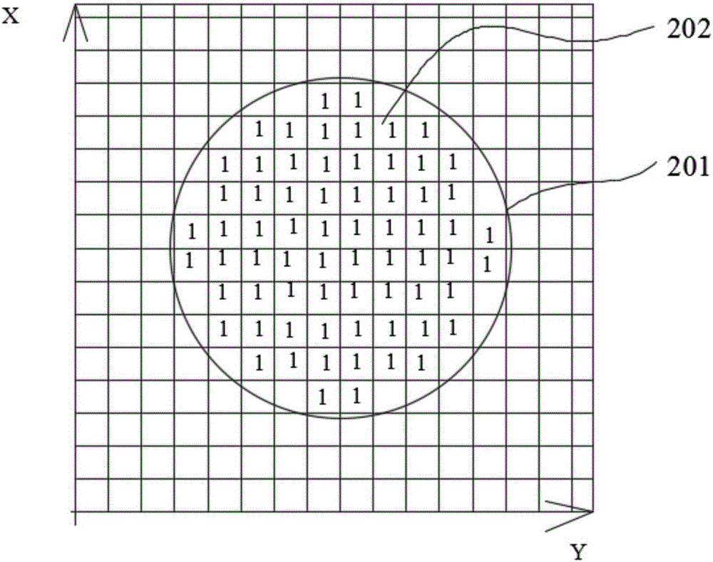
[0034] Such as image 3 As shown, the display mode of this embodiment is to draw a two-dimensional image 301 corresponding to the test wafer on the screen, and the chip passing coordinates of the test wafer are in one-to-one correspondence with the chip image 302 in the two-dimensional image, and the chip test passes , the corresponding chip image 302 is displayed in green; if the chip test fails, the corresponding chip image 302 is displayed in red. In this display mode, no specific items need to be selected. As long as one test item fails, the control unit 102 judges that the chip has failed the test, and controls the display and interaction unit to display red on the chip image 302 . It can be understood that other different colors can be used to represent the pass and fail of the chip test. Of course, in order to i...
Embodiment 3
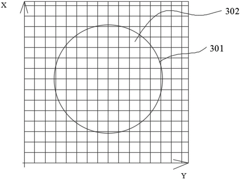
[0037] The difference between this embodiment and Embodiment 2 is that the display mode of the display and interaction unit 105 is that the control unit 102 superimposes two-dimensional images of a plurality of similar test wafers, and all chips with the same coordinates of the test wafers are If the test fails, the coordinate chip will display the specified color. This display mode can quickly analyze the common failure pattern of the wafer, so as to determine the failure cause of the test wafer. When the chip image is clicked by the mouse, the test information of all test items of a plurality of similar test wafers and the chip corresponding to the clicked chip image can also be displayed.
[0038] Using the wafer test system provided by the present invention, the control unit extracts the test data of the specified test wafer from the data storage unit according to the instructions received by the display and interaction unit, and controls the display and interaction unit t...
PUM
 Abstract
Description
Claims
Application Information