Display panel and display device

A technology for display panels and circuit boards, which is applied to static indicators, nonlinear optics, instruments, etc., can solve the problems of high and low production costs of display panels and display devices, and achieve high production costs and low production costs. cost effect

Active Publication Date: 2017-04-26
TCL CHINA STAR OPTOELECTRONICS TECH CO LTD
View PDF6 Cites 7 Cited by
  • Summary
  • Abstract
  • Description
  • Claims
  • Application Information

AI Technical Summary

Problems solved by technology

[0006] Embodiments of the present invention provide a display panel and a display device with relatively low production costs, so as to solve the technical problem of high production costs of existing display panels and display devices

Method used


Image

  • Display panel and display device
  • Display panel and display device
  • Display panel and display device

Examples


Embodiment Construction

[0029] The following descriptions of the various embodiments refer to the accompanying drawings to illustrate specific embodiments in which the present invention can be practiced. The directional terms mentioned in the present invention, such as "up", "down", "front", "back", "left", "right", "inside", "outside", "side", etc., are for reference only The orientation of the attached schema. Therefore, the directional terms used are used to illustrate and understand the present invention, but not to limit the present invention.

[0030] In the figures, structurally similar units are denoted by the same reference numerals.

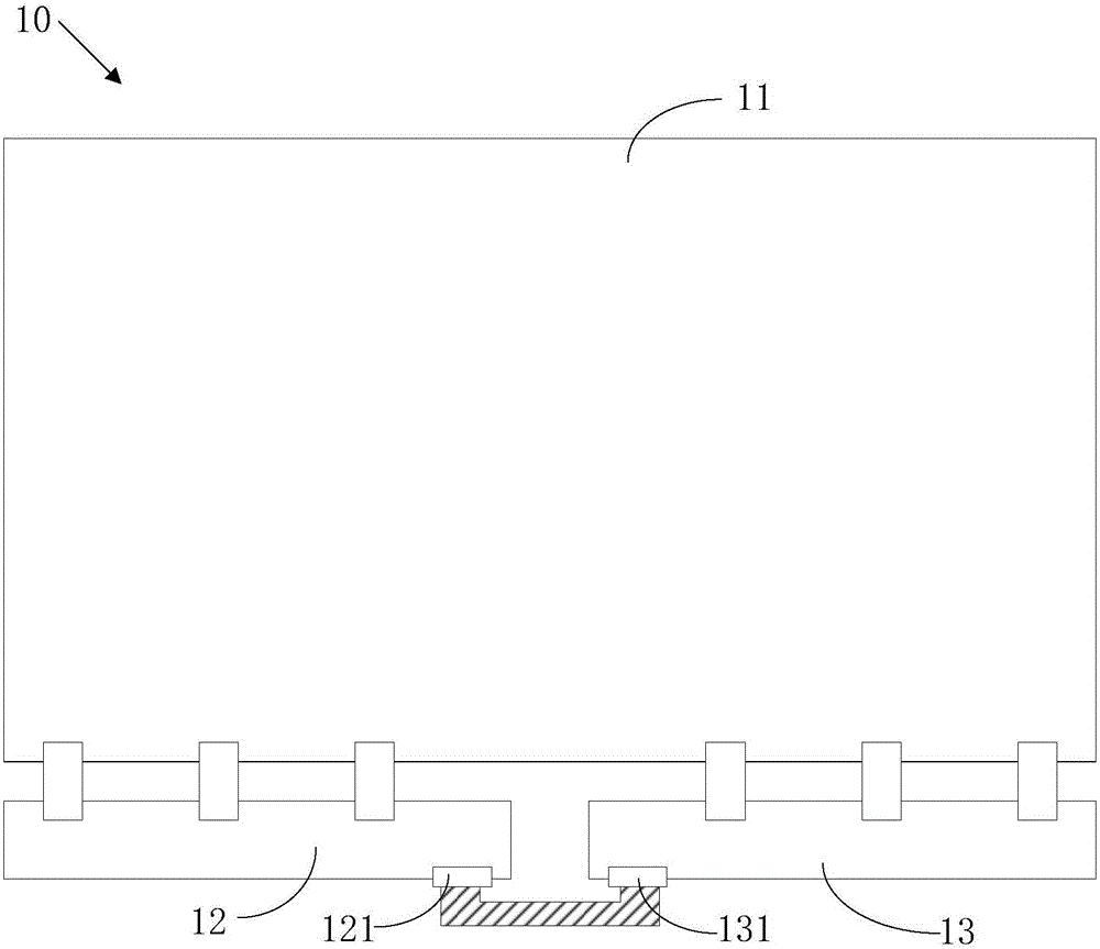
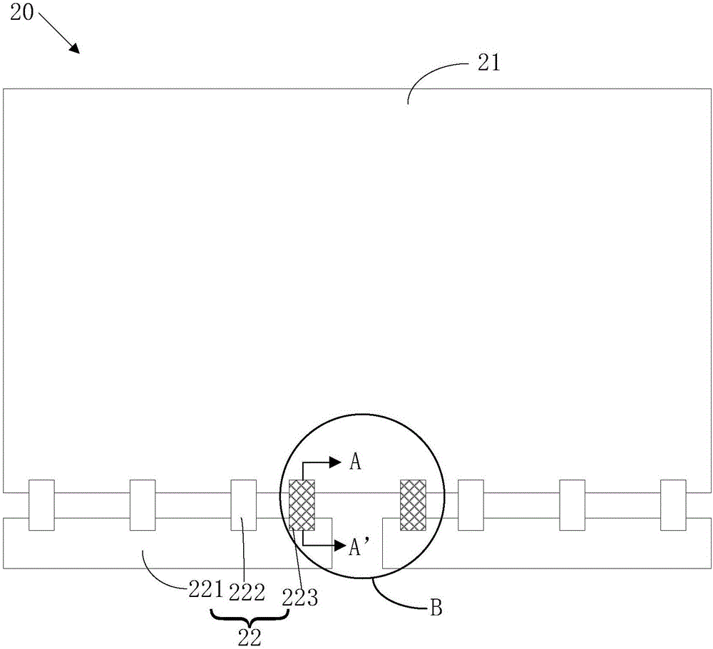
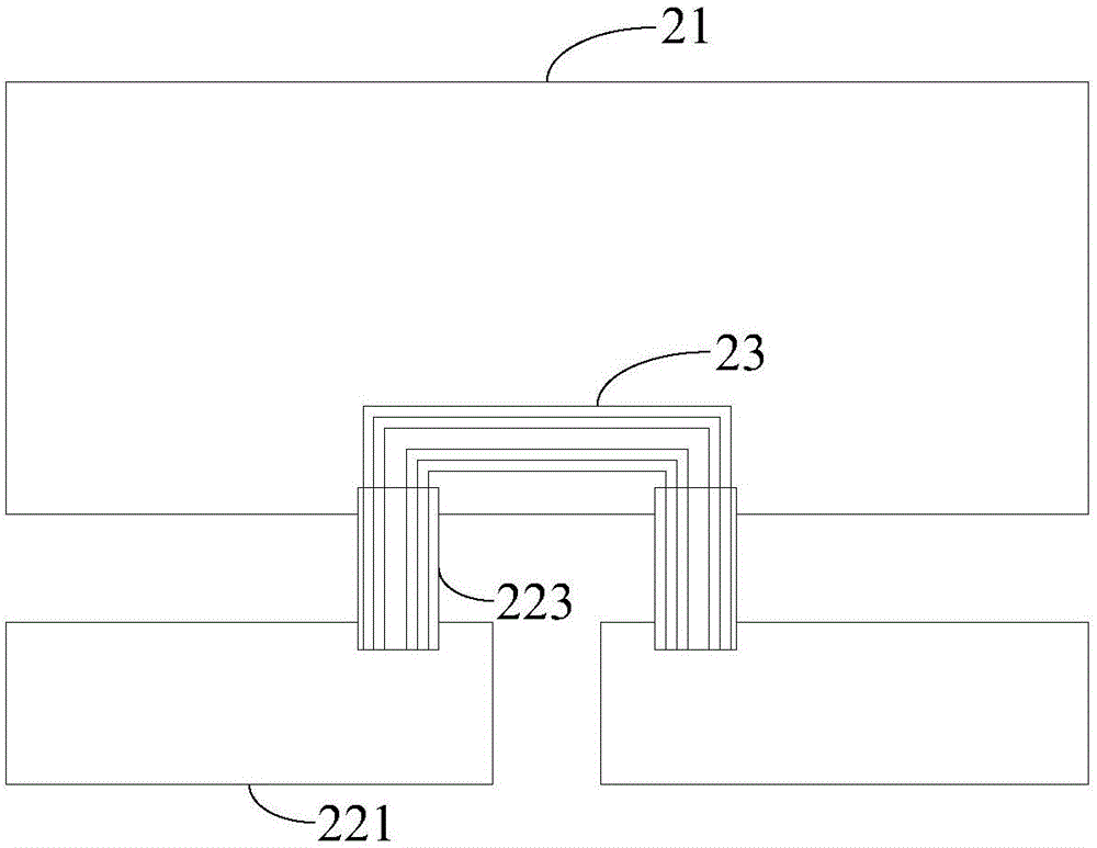
[0031] Please refer to Figure 2 to Figure 4 , Figure 2A is a schematic structural diagram of a preferred embodiment of the display panel of the present invention, Figure 2B for Figure 2A A magnified view of part B of the image 3 for Figure 2A The schematic diagram of the structure of the A-A' section, Figure 4 It is a schematic structural diagra...


PUM


Abstract

The invention provides a display panel which comprises a display panel body and at least two driving circuits. The display panel body comprises data wires, scanning wires, pixel units which are formed through intersection of the data wires and the scanning wires, and a circuit board wiring which is used for different driving circuit boards. Each driving circuit board comprises a circuit board body, a first bridging wire and a second bridging wire, wherein the second bridging wire is connected with the circuit board wiring on the display panel body and the circuit board body for transmitting a cascading signal. The first bridging wire is connected with the data wires and scanning wires on the display panel body, and the circuit board body and is used for transmitting a data signal and a scanning signal in response to the cascading signal. The invention further provides a display device. According to the display panel and the display device, different driving circuit boards are connected through the second bridging wire and the circuit board wiring, thereby reducing manufacturing cost of a driving circuit board connecting device and furthermore reducing manufacturing cost of the corresponding display panel.

Description

technical field [0001] The invention relates to the field of display driving, in particular to a display panel and a display device. Background technique [0002] Due to upgrading, the current display panel manufacturers are using larger and larger glass substrates, and the size of the display panels they produce is also increasing, such as 65 inches, 85 inches, and 110 inches. The larger the size of the display panel, the larger the area of ​​the driving circuit board used in conjunction with it. [0003] However, due to the limitation of the production process of the printed circuit board, the maximum size of the existing drive circuit board can only be about 600mm. Therefore, when the display panel is large in size, multiple drive circuit boards are often installed. For details, please refer to figure 1 , figure 1 It is a structural schematic diagram of an existing display panel. The display panel 10 includes a display panel main body 11 and a first driving circuit boa...

Claims


Application Information

Patent Timeline
Patent Type & Authority Applications(China)
IPC IPC(8): G09G3/20G02F1/1362
CPCG02F1/136286G09G3/20G09G2300/0426G02F1/13452G09G3/34
Inventor 陈宥烨陈胤宏胡安乐
Owner TCL CHINA STAR OPTOELECTRONICS TECH CO LTD
Why Eureka
Try Eureka