Chip monitoring device and method for flip-chip process

A chip mounting and chip technology, which is applied in the field of chip flip-chip process chip monitoring devices, can solve the problems of difficult positioning, undetectable damage, hidden dangers, etc., and achieves the effect of reducing production failure rate, precise control, and enhanced visibility.

Active Publication Date: 2020-02-21
BEIJING MXTRONICS CORP +1
View PDF3 Cites 0 Cited by
  • Summary
  • Abstract
  • Description
  • Claims
  • Application Information

AI Technical Summary

Problems solved by technology

[0002] Flip-chip technology is one of the important factors affecting the quality of flip-chip products. However, due to the characteristics of the flip-chip packaging process, the chip needs to be flipped and then mounted on the ceramic substrate. Point surface observation cannot guarantee the surface state of chips and bumps before flip-chip welding, and due to the characteristics of flip-chip packaging circuit bump surface array arrangement, it is impossible to directly perform visual inspection of solder joints after reflow soldering. The method is to inspect the chip and solder joints before flipping the chip, and carry out the follow-up process if the inspection is good.
However, if the chip or the bump is damaged during the chip flipping process, the damage in this process cannot be found, so there is a certain hidden danger
In addition, the traditional chip flip-chip equipment has the functions of mounting and welding, but does not have the function of observing and recording the chip process. If the circuit fails later, the original state of the chip and bumps cannot be traced, making it difficult to locate the failure problem.

Method used


Image

  • Chip monitoring device and method for flip-chip process
  • Chip monitoring device and method for flip-chip process
  • Chip monitoring device and method for flip-chip process

Examples


Embodiment Construction

[0033] Below in conjunction with accompanying drawing, the present invention will be described in further detail:

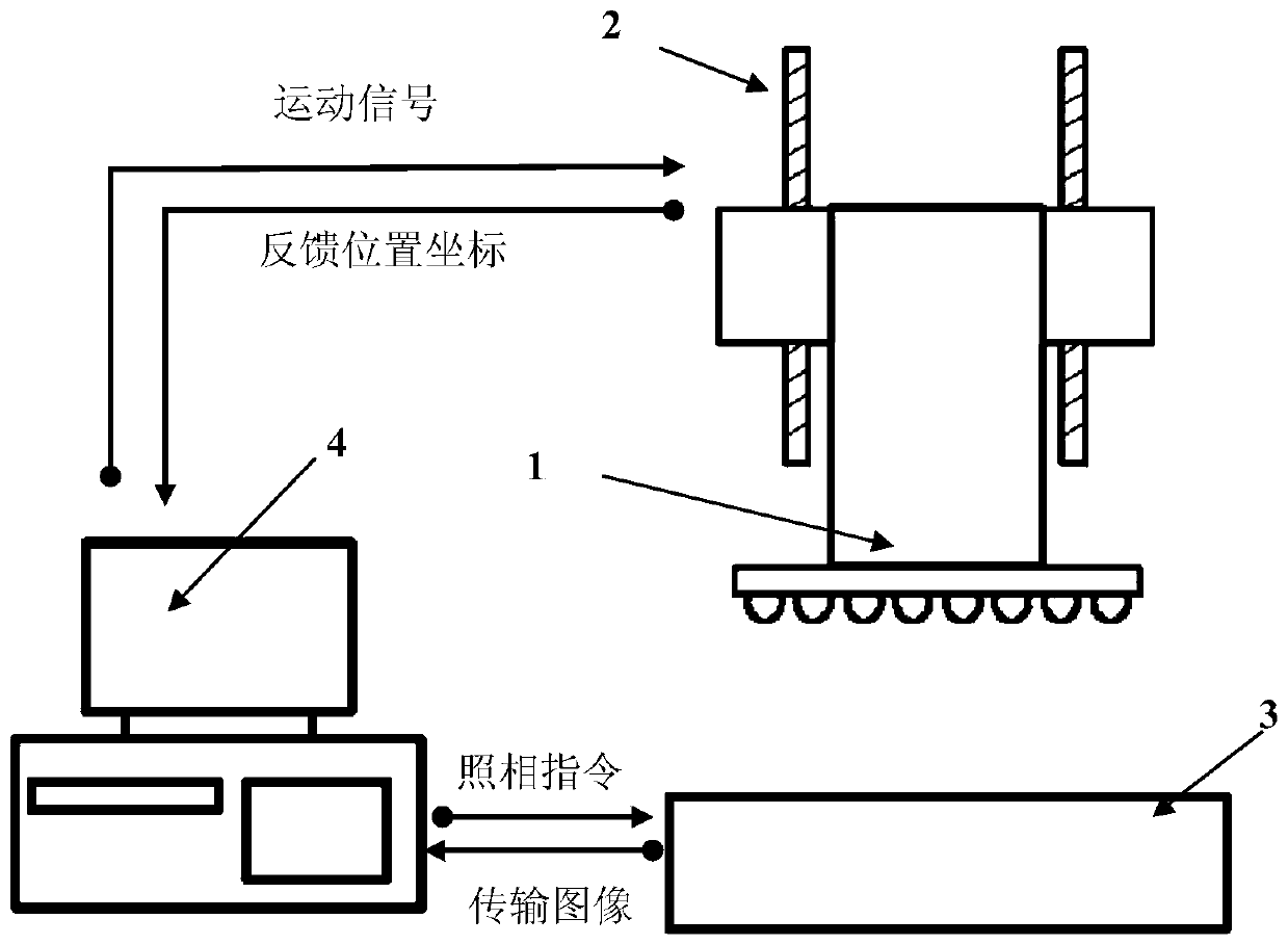
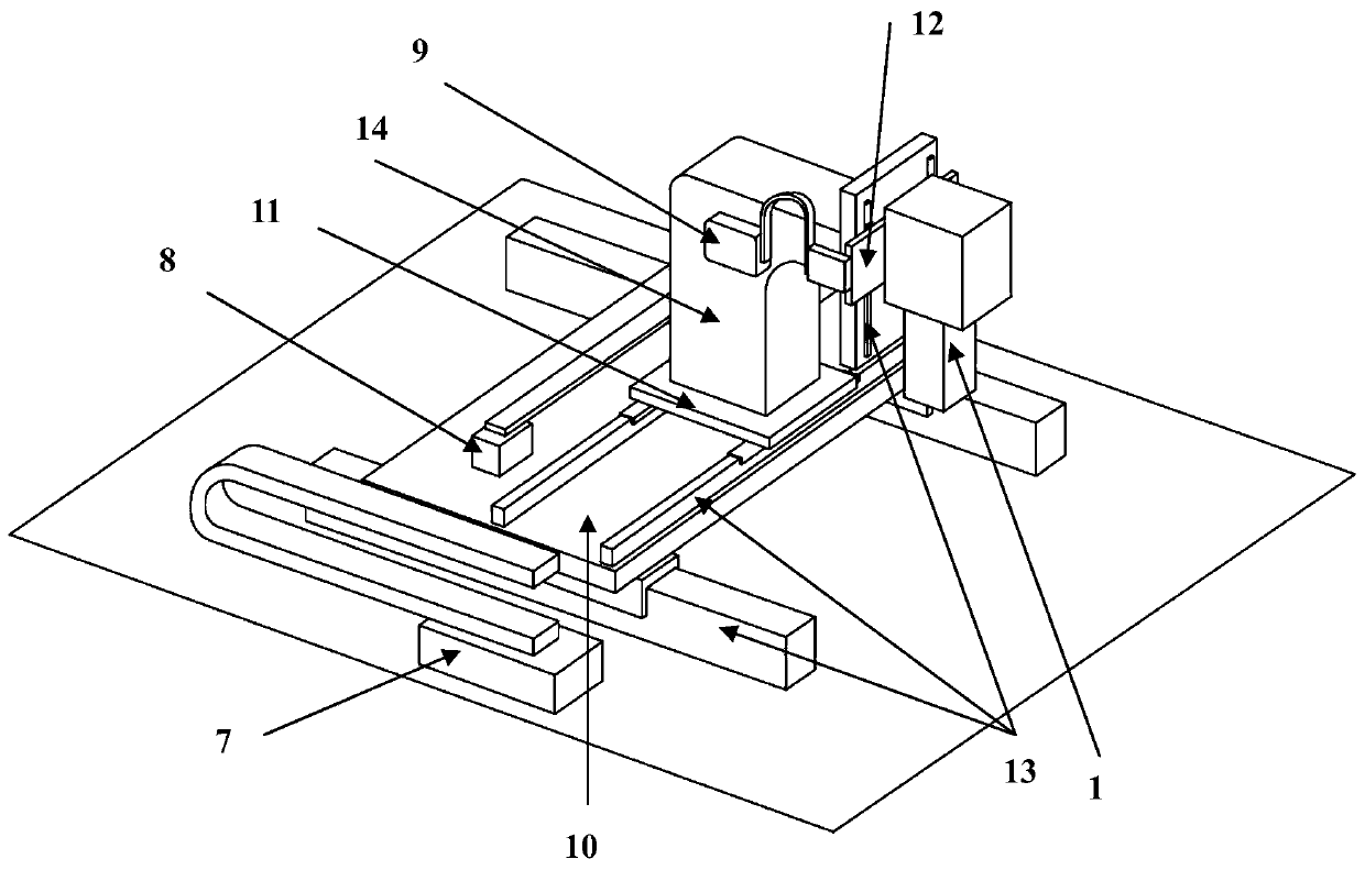
[0034] Such as figure 1 As shown, the present invention provides a chip monitoring device for a flip-chip process, which is composed of a chip mounting head 1 , a moving mechanism 2 , a photographing device 3 and a control computer 4 . in:

[0035] The chip mounting head 1 is vertically and fixedly installed on the moving mechanism 2, and is used for absorbing chips with bumps;

[0036] The moving mechanism 2, driven by the motion control signal of the control computer 4, drives the chip placement head 1 to move horizontally or vertically;

[0037] The photographing device 3 is fixedly placed on a horizontal plane, and its photographing camera faces vertically upwards, receives the amplification control signal sent by the control computer 4, takes pictures of the bump surface of the chip according to the amplification control signal, obtains the image informati...


PUM


Abstract

The invention discloses a chip monitoring device and a chip monitoring method for a chip upside-down mounting process. The method comprises the following steps: the feature point image information of a bumped chip is preloaded to a control computer; the bumped chip is inverted and mounted on a chip surface mounting head by adsorption; the control computer sends a control signal according to the position information of a mobile mechanism and the chip surface mounting head to make the chip within the visual range of a shooting device, wherein the camera of the shooting device focuses on the tested bumped chip; the image information of the bumped surface of the bumped chip is acquired, the feature points in the image information are identified, a motion control signal is sent to the mobile mechanism, and the position of the chip surface mounting head is adjusted to make the feature points fit a preset feature point image; the bumped surface image information shot at the moment is stored; and whether the chip is usable is judged, and the judgment result is output and displayed. It is ensured that chips used in a chip upside-down mounting process are good. The use of bad chips, such as damaged chips and chips with damaged balls, is reduced. The control power for raw materials of devices is improved significantly.

Description

technical field [0001] The invention relates to a chip monitoring device and method for chip flip chip technology, which is suitable for flip chip flip chip technology process. Background technique [0002] Flip-chip technology is one of the important factors affecting the quality of flip-chip products. However, due to the characteristics of the flip-chip packaging process, the chip needs to be flipped and then mounted on the ceramic substrate. Point surface observation cannot guarantee the surface state of chips and bumps before flip-chip welding, and due to the characteristics of flip-chip packaging circuit bump surface array arrangement, it is impossible to directly perform visual inspection of solder joints after reflow soldering. The method is to inspect the chips and solder joints before flipping the chips, and carry out the follow-up process if the inspection is good. However, if the chip or the bump is damaged during the chip flipping process, the damage in this pro...

Claims


Application Information

Patent Timeline
Patent Type & Authority Patents(China)
IPC IPC(8): H01L21/67
CPCH01L21/67253H01L21/67288
Inventor 姜学明姚全斌王勇练滨浩林鹏荣黄颖卓刘建松
Owner BEIJING MXTRONICS CORP
Why Eureka
Try Eureka