
Preparation method of silicon carbide surface oxidation film

A surface oxidation and silicon carbide technology, which is applied in semiconductor/solid-state device manufacturing, electrical components, circuits, etc., can solve the problems of SiC MOSFET device performance degradation, complex oxidation mechanism, etc., to reduce interface state density, simple process, and improve quality Effect

Active Publication Date: 2017-05-03
GLOBAL ENERGY INTERCONNECTION RES INST CO LTD +2
View PDF3 Cites 2 Cited by
  • Summary
  • Abstract
  • Description
  • Claims
  • Application Information

AI Technical Summary

Problems solved by technology

[0003] However, due to the presence of C, the oxidation mechanism of silicon carbide is much more complicated than that of silicon, and the interface state densit

Method used


Image

  • Preparation method of silicon carbide surface oxidation film
  • Preparation method of silicon carbide surface oxidation film
  • Preparation method of silicon carbide surface oxidation film

Examples


Example Embodiment

[0030] Example 1

[0031] A method for preparing an oxide film on a silicon carbide surface, the method comprising the steps of:

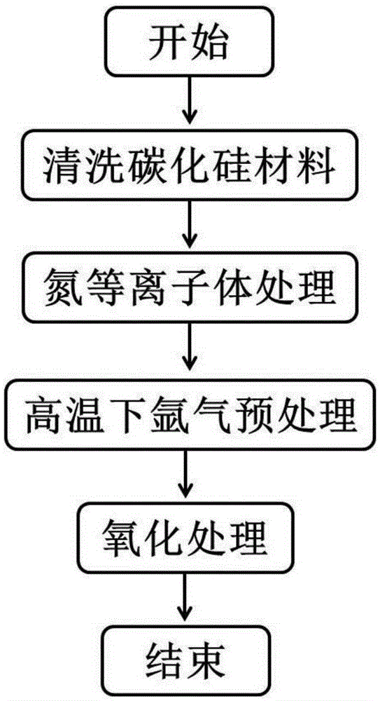
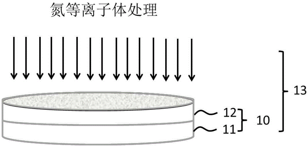
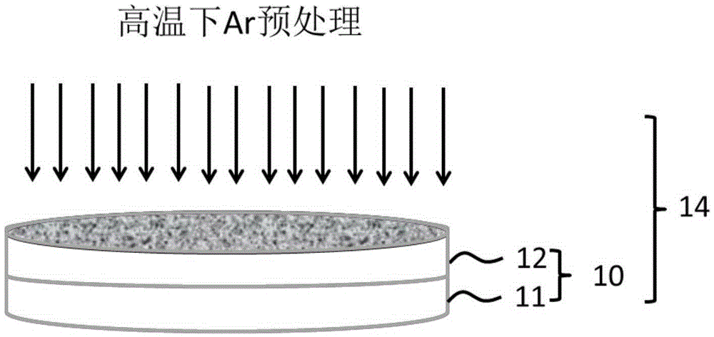
[0032] 1) Clean the silicon carbide material 10, the silicon carbide material 10 includes a substrate 11 and an epitaxial film 12, the substrate 11 in the silicon carbide material 10 is n-type 4H-SiC, the thickness is about 380 μm, n-type doped impurities Nitrogen (N), the doping concentration is about 5×10 18 cm -3 ; The epitaxial film 12 in the silicon carbide material 10 is n-type 4H-SiC with a thickness of about 12 μm, and the n-type doped impurity is nitrogen (N), and the doping concentration is about 8×10 15 cm -3 ;

[0033] The silicon carbide material 10 is cleaned by the RCA standard cleaning method, and the specific cleaning steps are as follows:

[0034] (1) Prepare hydrofluoric acid solution (HF:H 2 O=1:10);

[0035] (2) The sample holder is cleaned and dried for use;

[0036] (3) Take the silicon carbide sample 10 and put it on...

Example Embodiment

[0048] Example 2

[0049] A method for preparing an oxide film on a silicon carbide surface, the method comprising the steps of:

[0050]1) Clean the silicon carbide material 10, the silicon carbide material 10 includes a substrate 11 and an epitaxial film 12, the substrate 11 in the silicon carbide material 10 is n-type 4H-SiC, the thickness is about 300 μm, n-type doped impurities Nitrogen (N), the doping concentration is about 5×10 20 cm -3 ; The epitaxial film 12 in the silicon carbide material 10 is n-type 4H-SiC with a thickness of about 15 μm, and the n-type doped impurity is nitrogen (N), and the doping concentration is about 8×10 18 cm -3 ;

[0051] The silicon carbide material 10 is cleaned by the RCA standard cleaning method, and the specific cleaning steps are as follows:

[0052] (1) Prepare hydrofluoric acid solution (HF:H 2 O=1:10);

[0053] (2) The sample holder is cleaned and dried for use;

[0054] (3) Take the silicon carbide sample 10 and put it on ...

Example Embodiment

[0066] Example 3

[0067] A method for preparing an oxide film on a silicon carbide surface, the method comprising the steps of:

[0068] 1) Cleaning the silicon carbide material 10, the silicon carbide material 10 includes a substrate 11 and an epitaxial film 12, the substrate 11 in the silicon carbide material 10 is n-type 6H-SiC, the thickness is about 450 μm, n-type doped impurities Nitrogen (N), the doping concentration is about 5×10 18 cm -3 ; The epitaxial thin film 12 in the silicon carbide material 10 is n-type 6H-SiC, the thickness is about 15 μm, the n-type doping impurity is nitrogen (N), and the doping concentration is about 8×10 15 cm -3 ;

[0069] The silicon carbide material 10 is cleaned by the RCA standard cleaning method, and the specific cleaning steps are as follows:

[0070] (1) Prepare hydrofluoric acid solution (HF:H 2 O=1:10);

[0071] (2) The sample holder is cleaned and dried for use;

[0072] (3) Take the silicon carbide sample 10 and put it...


PUM

PropertyMeasurementUnit
Thicknessaaaaaaaaaa
Doping concentrationaaaaaaaaaa

Abstract

The invention discloses a preparation method of a silicon carbide surface oxidation film. The method comprises the following steps that 1) a silicon carbide material (10) including a substrate (11) and an epitaxial film (12) is cleaned; 2) nitrogen plasma processing is carried out on the upper surface of the epitaxial film (12); 3) a sample (13) obtained in the step 2) is preprocessed by argon at high temperature; and 4) a sample (14) obtained in the step 3) is oxidized to obtain the oxidation film (15). Passivation is carried out on the surface of silicon carbide before that the silicon carbide oxidation film is formed, the quality of the silicon carbide oxidation film is improved, the interface state density of silicon carbide/silica is reduced, and the method is easy to carry out, and suitable for large-scale industrial production.

Description

technical field [0001] The invention relates to a method for processing semiconductor materials, in particular to a method for preparing an oxide film on the surface of silicon carbide. Background technique [0002] Silicon carbide materials have the characteristics of wide band gap, high breakdown field strength, high thermal conductivity, high saturation electron mobility, excellent physical and chemical stability, and are suitable for high temperature, high frequency, high power and extreme environments. Silicon carbide is the only one that can generate SiO by thermal oxidation 2 The wide bandgap semiconductor of the dielectric layer makes silicon carbide especially suitable for the preparation of various MOS structure devices. [0003] However, due to the presence of C, the oxidation mechanism of silicon carbide is much more complicated than that of silicon, and the interface state density of silicon carbide / silicon dioxide is much higher than that of silicon / silicon di...

Claims


Application Information

Patent Timeline
IPC IPC(8): H01L21/02
CPCH01L21/02164H01L21/0223H01L21/02312H01L21/02315
Inventor 郑柳杨霏王方方李玲李永平朱韫晖夏经华田亮查祎英李嘉琳
Owner GLOBAL ENERGY INTERCONNECTION RES INST CO LTD
Learn More