IBIS-based integrated circuit total dose effect modeling method

A technology of total dose effect and modeling method, applied in the field of IBIS-based integrated circuit total dose effect modeling, which can solve problems such as simulation analysis of signal integrity problems

Inactive Publication Date: 2017-05-10
XIDIAN UNIV
View PDF3 Cites 5 Cited by
  • Summary
  • Abstract
  • Description
  • Claims
  • Application Information

AI Technical Summary

Problems solved by technology

[0004] The purpose of the present invention is to provide a method for modeling the total dose effect of integrated circuits based on IBIS, aiming to solve the problem that the existing signal integrity simulation software can only give the signal integrity of PCB under conventional conditions (no irradiation conditions). Analysis strategy, but unable to simulate the signal integrity problem of PCB in the case of total dose effect

Method used


Image

  • IBIS-based integrated circuit total dose effect modeling method
  • IBIS-based integrated circuit total dose effect modeling method
  • IBIS-based integrated circuit total dose effect modeling method

Examples


Embodiment Construction

[0024] In order to make the object, technical solution and advantages of the present invention more clear, the present invention will be further described in detail below in conjunction with the examples. It should be understood that the specific embodiments described here are only used to explain the present invention, not to limit the present invention.

[0025] The application principle of the present invention will be described in detail below in conjunction with the accompanying drawings.

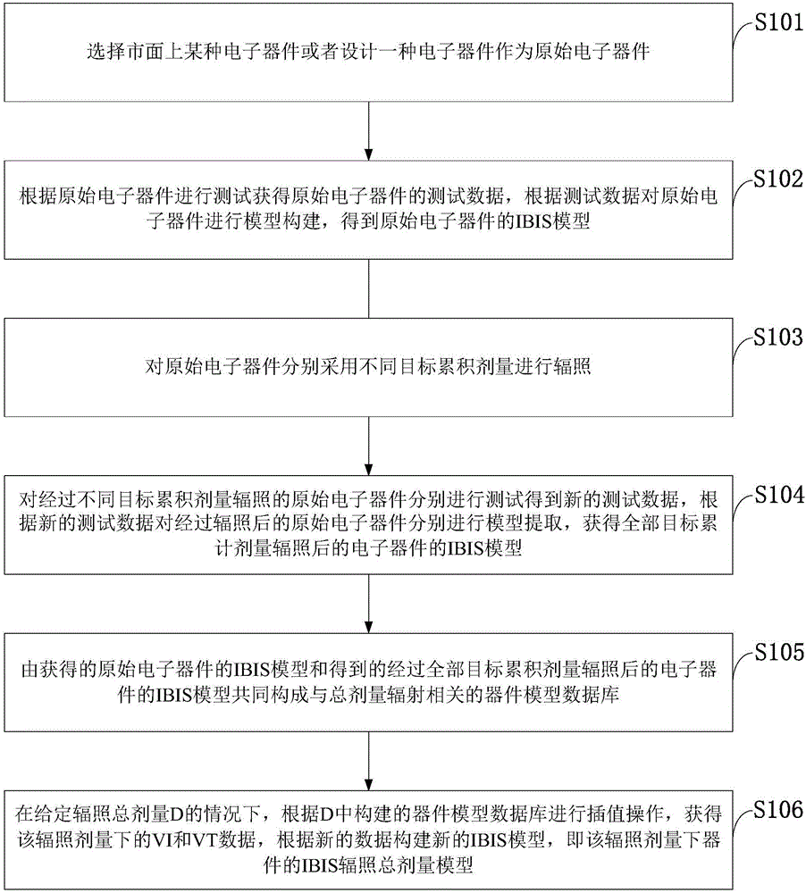
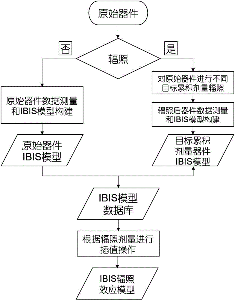
[0026] Such as figure 1 As shown, the IBIS-based integrated circuit total dose effect modeling method provided by the embodiment of the present invention includes the following steps:

[0027] S101: Select an electronic device on the market or design an electronic device as the original electronic device;

[0028] S102: Perform testing according to the original electronic device to obtain test data of the original electronic device, construct a model of the original electronic device...


PUM


Abstract

The invention discloses an IBIS-based integrated circuit total dose effect modeling method. The IBIS-based integrated circuit total dose effect modeling method comprises the steps of performing irradiation on an original electronic device by adopting different target accumulated doses; performing data measurement and model extraction on the irradiated original electronic device, and establishing an IBIS model database of the electronic device under all the target accumulated doses; under the condition of giving a total irradiation dose D, performing interpolation operation on the established model database of the device according to the total irradiation dose D to obtain VI and VT interpolation data under the irradiation dose, and building an IBIS model according to the interpolation data, namely, an IBIS irradiation total dose effect model of the device under the irradiation dose. According to the method, the influence of irradiation conditions on PCB signal integrity is considered based on original PCB signal integrity analysis, and model support is provided for performing simulation analysis of PCB signal integrity problem under the irradiation condition.

Description

technical field [0001] The invention belongs to the technical field of modeling of device radiation effect models, in particular to an IBIS-based method for modeling the total dose effect of integrated circuits. Background technique [0002] At present, in order to meet people's requirements for miniaturization and multi-function of electronic equipment, the printed circuit board (PCB) is developing towards high speed, high density and high integration. When the signal rate and component density increase to a certain level, the parasitic effect on the PCB will cause noise and interference on the transmission signal, and the PCB will not work well. This requires good signal integrity simulation design in the PCB design stage of electronic product development. The device model used in simulation will directly affect the accuracy of simulation. The device model widely used in signal integrity simulation in the industry is the IBIS model (a method for quickly and accurately mo...

Claims


Application Information

Patent Timeline
Patent Type & Authority Applications(China)
IPC IPC(8): G06F17/50
CPCG06F30/39
Inventor 王泉刘太彬刘锦辉李静月刘刚
Owner XIDIAN UNIV
Why Eureka
Try Eureka