Thin film transistor and its preparation method, array substrate, display device

A technology of thin film transistors and array substrates, applied in the display field, can solve problems such as poor switch reliability, and achieve the effect of improving poor coverage

Active Publication Date: 2020-04-28
CHENGDU VISTAR OPTEOLECTRONICS CO LTD
View PDF5 Cites 0 Cited by
  • Summary
  • Abstract
  • Description
  • Claims
  • Application Information

AI Technical Summary

Problems solved by technology

This situation leads to poor switching reliability of existing thin-film transistors

Method used


Image

  • Thin film transistor and its preparation method, array substrate, display device
  • Thin film transistor and its preparation method, array substrate, display device
  • Thin film transistor and its preparation method, array substrate, display device

Examples


Embodiment Construction

[0037] In order to enable those skilled in the art to better understand the technical solutions in the present invention, the technical solutions in the embodiments of the present invention will be clearly and completely described below in conjunction with the drawings in the embodiments of the present invention. Obviously, the described The embodiments are only some of the embodiments of the present invention, not all of them. Based on the embodiments of the present invention, all other embodiments obtained by persons of ordinary skill in the art without making creative efforts shall fall within the protection scope of the present invention.

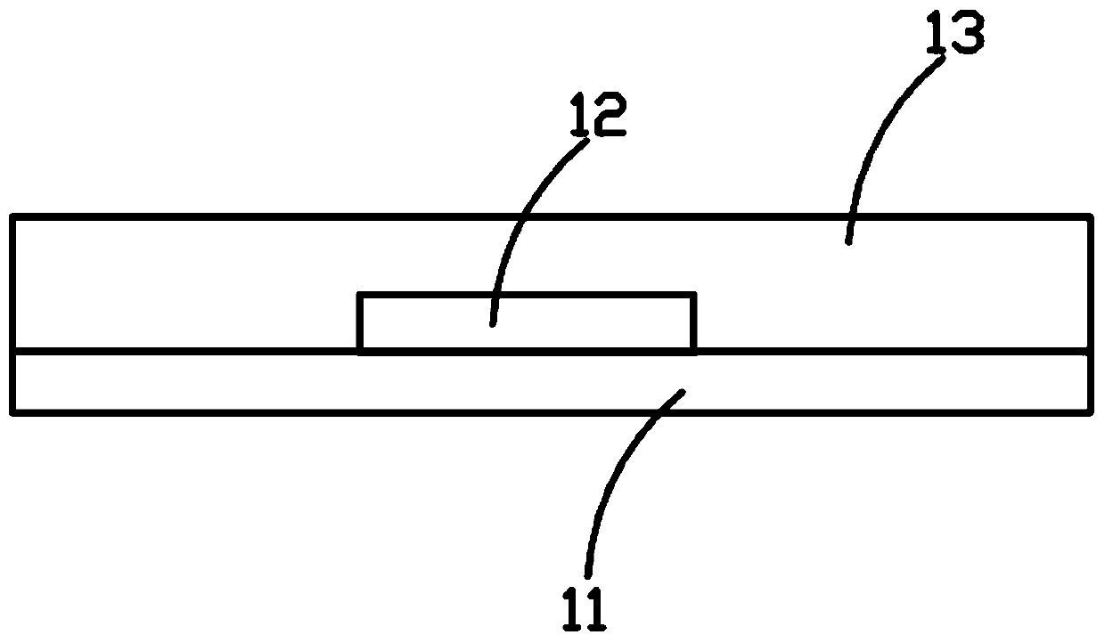
[0038] Secondly, in describing the embodiments of the present invention in detail, for the convenience of explanation, the cross-sectional view showing the structure of the thin film transistor will not be partially enlarged according to the general scale, and the drawings are only examples, which should not limit the protection of the p...


PUM


Abstract

The embodiment of the invention discloses a preparation method of a thin-film transistor, the thin-film transistor prepared by the method, an array substrate of using the thin-film transistor and display equipment of using the array substrate. The method comprises the steps as follows: a substrate is provided; an active layer with a preset shape is formed on the surface of one side of the substrate; the surface of the active layer is provided with a photoresist layer for etching; an auxiliary insulating layer is formed on the peripheral side of the active layer; and a gate insulating layer is formed on the surfaces of the auxiliary insulating layer and the active layer. The auxiliary insulating layer is added to the peripheral side of the active layer, so that the covering property of the gate insulating layer on the peripheral side of the active layer is relatively good, and the problem of poor device reliability caused by poor covering property of the gate insulating layer is effectively solved.

Description

technical field [0001] The invention relates to the field of display technology, in particular to a method for preparing a thin film transistor, a thin film transistor prepared by the method, an array substrate using the thin film transistor, and a display device using the array substrate. Background technique [0002] Thin-film transistors (Thin-film transistors, TFTs) are currently widely used in display devices due to their good switching characteristics. [0003] Such as figure 1 As shown, the structure of the existing thin film transistor generally includes a substrate 11, an active layer 12 and a gate insulating layer 13. The active layer 12 is formed on the upper surface of the substrate, and the gate insulating layer 13 covers the active layer 12 and part of the Substrate 11. [0004] However, in figure 1 In the thin film transistor shown, since the coverage of the gate insulating layer 13 on the edge of the active layer is poor, the film layer on the edge of the ...

Claims


Application Information

Patent Timeline
Patent Type & Authority Patents(China)
IPC IPC(8): H01L21/77H01L27/12
CPCH01L27/1214H01L27/1248H01L27/1259
Inventor 徐琳袁波高胜
Owner CHENGDU VISTAR OPTEOLECTRONICS CO LTD
Why Eureka
Try Eureka