Bonding pad structure for encapsulating full color lamp bead of COB panel

A disk structure and pad technology, applied in electrical components, electrical solid devices, circuits, etc., can solve the problems of unstable display screen, unstable full-color COB panel lamp beads, etc., and achieve stable packaging, large light-emitting angle, and color mixing. uniform effect

Pending Publication Date: 2017-05-10
SHENZHEN AUROLED TECH
View PDF4 Cites 1 Cited by
  • Summary
  • Abstract
  • Description
  • Claims
  • Application Information

AI Technical Summary

Problems solved by technology

[0004] In view of the technical problem that the pad structure in the prior art is likely to cause instability of the display screen, it is necessary to provide a full-color COB panel lamp bead packaging pad structure that is not easy to cause instability

Method used


Image

  • Bonding pad structure for encapsulating full color lamp bead of COB panel
  • Bonding pad structure for encapsulating full color lamp bead of COB panel

Examples


Embodiment Construction

[0012] Now in conjunction with the accompanying drawings, the preferred embodiments of the present invention will be described in detail.

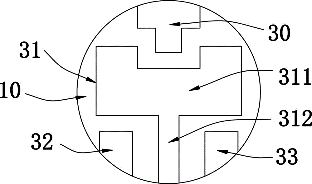
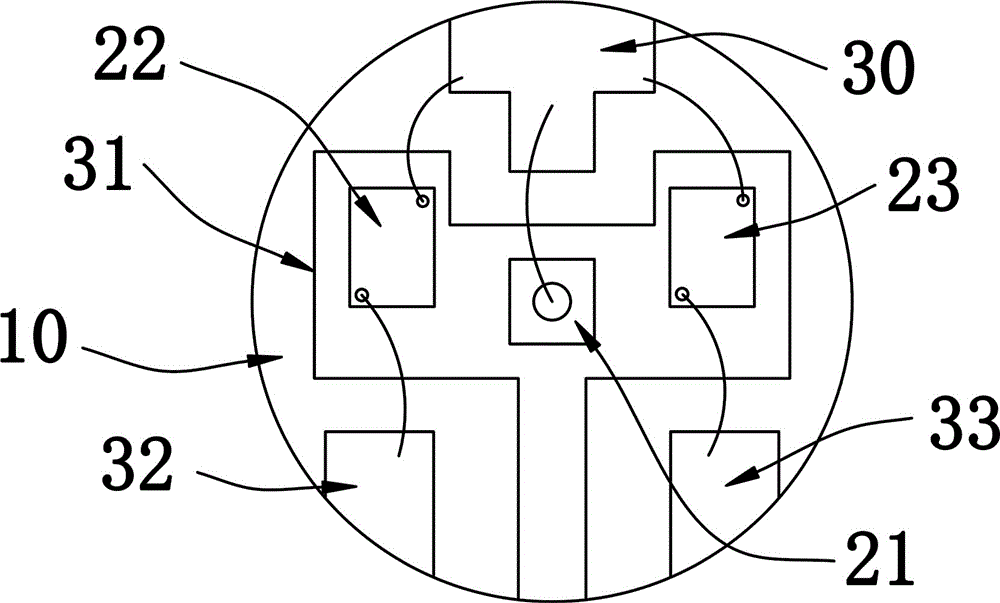
[0013] The invention proposes a full-color COB panel lamp bead packaging pad structure. see figure 1 , including the lamp cup 10, the first pad 31, the second pad 32, the third pad 33, the fourth pad 30, the first wafer 21, the second wafer 22 and the third wafer 23; the lamp cup 10 is round shape, the first pad 31, the second pad 32, the third pad 33, and the fourth pad 30 are all set in the lamp cup 10, the first pad 31 is in the shape of a "T", and is formed by the cross arm 311 and the vertical The cross arm 311 and the vertical arm 312 are located on one diameter of the lamp cup 10, the second welding pad 32 is located on one side of the vertical arm 312, and the third welding pad 33 is located on the side of the vertical arm 312 relative to the second welding pad 32. On the other side, the fourth pad 30 is located on the side of th...


PUM


Abstract

The invention relates to a bonding pad structure for encapsulating a full color lamp bead of a COB panel. The bonding pad structure for encapsulating the full color lamp bead of the COB panel comprises a lamp cup, a first bonding pad, a second bonding pad, a third bonding pad, a fourth bonding pad, a first wafer, a second wafer and a third wafer, wherein the lamp cup is round; the first bonding pad, the second bonding pad, the third bonding pad and the fourth bonding pad are all arranged in the lamp cup; the first bonding pad is T-shaped and is formed by a cross arm and a vertical arm; the cross arm and the vertical arm are arranged on one diameter of the lamp cup; the second bonding pad is arranged at one side of the vertical arm; the third bonding pad is arranged on the other side of the vertical arm relative to the second bonding pad; and the fourth bonding pad is arranged at one side of the cross arm, which is far away from the vertical arm. According to the bonding pad structure, the encapsulation of the full color lamp bead of the COB panel is more stable, the color mixture is uniform and the emitting angle is larger.

Description

technical field [0001] The invention relates to an LED lamp bead structure, in particular to a full-color small-pitch COB panel lamp bead packaging pad structure. Background technique [0002] Traditional small light-emitting diodes have a relatively small space for the solder pads of the crystal lamp cup, and because the size of the LED lamp bead is small, it affects its own stability. At the same time, the solder feet are fine and tight, which seriously affects the processing difficulty and reliability of the LED panel. , Therefore, a single LED lamp bead is a limiting factor for the small pitch of the LED display. [0003] At present, COB panels have appeared on the market to replace traditional small light-emitting diodes, and it is easier to realize the small-pitch LED display. However, the lamp beads on the COB panel are limited by the processing procedures, and it is impossible to achieve mixed lights and other processes. This makes the packaging requirements of COB ...

Claims


Application Information

Patent Timeline
Patent Type & Authority Applications(China)
IPC IPC(8): H01L23/49H01L23/528H01L25/075
CPCH01L23/528H01L25/0753H01L23/49H01L2224/48091H01L2924/00014
Inventor 蒋顺才
Owner SHENZHEN AUROLED TECH
Why Eureka
Try Eureka