Eureka AIR delivers breakthrough ideas for toughest innovation challenges, trusted by R&D personnel around the world.

Nanoimprint shielding glass and manufacturing method therefor

A technology of shielding glass and nano-imprinting, applied in the fields of magnetic field/electric field shielding, electrical components, etc., can solve the problems of low product utilization, screen effect dependence, electronic equipment interference, etc., to achieve good effect and easy use.

Active Publication Date: 2017-05-10
索曼电子(深圳)有限公司
View PDF11 Cites 0 Cited by
  • Summary
  • Abstract
  • Description
  • Claims
  • Application Information

AI Technical Summary

Problems solved by technology

[0004] In recent years, with the extensive application of electronic and electrical equipment, electromagnetic waves propagate in space, causing mutual interference and information leakage of electronic equipment. In this case, it is easy to bring wrong actions and information of electronic equipment and automatic control systems. Being plagiarized while causing harm to people
[0005] Shielding glass can shield signals to ensure the safety of electronic and electrical equipment. Traditional shielding glass is mainly made of glass and wire mesh. Metal mesh is an imported product that needs to be blackened. The cost of the product is very high. The screen effect mainly depends on the imported network, and there is little room for improvement in product performance
In addition, the metal mesh and the display screen have an angle requirement, otherwise moiré patterns will be generated, so that the utilization rate of the product is lower

Method used


Image

  • Nanoimprint shielding glass and manufacturing method therefor
  • Nanoimprint shielding glass and manufacturing method therefor

Examples


Embodiment Construction

[0028] In order to make the object, technical solution and advantages of the present invention clearer, the present invention will be further described in detail below in conjunction with the accompanying drawings and embodiments. It should be understood that the specific embodiments described here are only used to explain the present invention, not to limit the present invention.

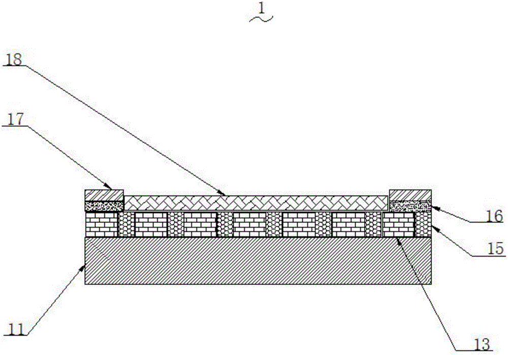
[0029] see figure 1 and figure 2 , a nano-imprinted shielding glass 1 of the present invention includes a plexiglass substrate 11, a low-viscosity monomer substrate layer 15 formed on the plexiglass substrate 11 and pre-imprinted with pattern grooves, and a low-viscosity monomer substrate layer 15 formed on the low-viscosity monomer substrate. The insulating layer 18 on the bottom layer 15; the conductive silver paste layer 16 and the conductive material layer 17 formed on the conductive silver paste layer 16 are arranged around the outside of the low viscosity monomer substrate layer 15; The na...


PUM

PropertyMeasurementUnit
thicknessaaaaaaaaaa
thicknessaaaaaaaaaa
thicknessaaaaaaaaaa

Abstract

The invention provides nanoimprint shielding glass and a manufacturing method therefor. The nanoimprint shielding glass comprises an organic glass substrate, a low-viscosity monomer substrate layer which is formed on the organic glass substrate and pre-imprinted with a pattern groove, and an insulating layer, wherein a conductive silver slurry layer and an conductive material layer formed on the conductive silver slurry layer are arranged on the periphery of the outer side of the low-viscosity monomer substrate layer; and a nano conductive layer corresponding to a pattern shape is arranged in the pattern groove of the low-viscosity monomer substrate layer. By forming the nano conductive layer matched with the groove pattern on the organic glass substrate, and by directly manufacturing a metal grid shielding layer on the glass through a nanoimprint technology, the screen effect, light transmittance and angle of the product all can be adjusted according to actual demands; the conductive silver slurry layer and the conductive material layer are arranged on the periphery of the outer side of the low-viscosity monomer substrate layer, so that metal net extension is avoided in such design; and therefore, only the conductive material which is connected with the shell is needed on the edge of the organic glass substrate; and the product usage is simpler and better in effect.

Description

[0001] [technical field] [0002] The invention relates to the technical field of glass production and manufacturing methods, in particular to a nano-imprinted shielding glass that can flexibly adjust the screen effect, light transmittance, angle and other characteristics of a product and a manufacturing method thereof. [0003] [Background technique] [0004] In recent years, with the extensive application of electronic and electrical equipment, electromagnetic waves propagate in space, causing mutual interference and information leakage of electronic equipment. In this case, it is easy to bring wrong actions and information of electronic equipment and automatic control systems. Being plagiarized and causing harm to people at the same time. [0005] Shielding glass can shield signals to ensure the safety of electronic and electrical equipment. Traditional shielding glass is mainly made of glass and wire mesh. Metal mesh is an imported product that needs to be blackened. The co...

Claims


Application Information

Patent Timeline
Patent Type & Authority Applications(China)
IPC IPC(8): H05K9/00
CPCH05K9/0086
Inventor 刘振栋
Owner 索曼电子(深圳)有限公司
Why Eureka
Eureka Blog
Learn More