Supercharge Your Innovation With Domain-Expert AI Agents!

Impedance matching device for reducing reflection loss by splitting digital signal and test system having the same

一种阻抗匹配、测试系统的技术,应用在自动化测试系统、单个半导体器件测试、波导型器件等方向,能够解决功耗温度增大等问题

Active Publication Date: 2017-05-17
SAMSUNG ELECTRONICS CO LTD
View PDF10 Cites 6 Cited by
  • Summary
  • Abstract
  • Description
  • Claims
  • Application Information

AI Technical Summary

Problems solved by technology

However, the use of active components results in increased power consumption and / or temperature

Method used


Image

  • Impedance matching device for reducing reflection loss by splitting digital signal and test system having the same
  • Impedance matching device for reducing reflection loss by splitting digital signal and test system having the same
  • Impedance matching device for reducing reflection loss by splitting digital signal and test system having the same

Examples


Embodiment Construction

[0023] Hereinafter, example embodiments of the inventive concept will now be described more fully so that those skilled in the art can easily understand the inventive concept.

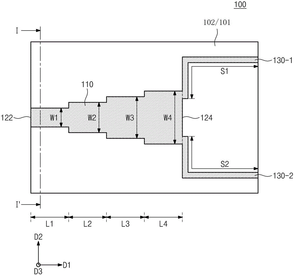
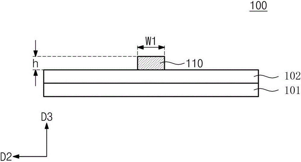
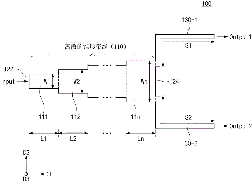
[0024] figure 1 is a plan view illustrating an impedance matching device 100 according to example embodiments of inventive concepts. refer to figure 1 , the impedance matching device 100 may include a tapered strip line 110 and a plurality of strip lines 130-1 and 130-2. exist figure 1 In , an impedance matching device 100 is shown disposed on a substrate and a dielectric layer.

[0025] The tapered stripline 110 may be arranged to extend in a first direction D1, and may have a width in a second direction D2 perpendicular to the first direction D1. The tapered stripline 110 may have a first end 122 through which a signal (for example, a digital signal) is input from an external device and a second end 124 that is the tapered stripline 110. Portions in contact with strip lines 130-1 and 130-2. In ...


PUM


Abstract

An impedance matching device includes a tapered strip line and a plurality of strip lines. The tapered strip line extends in a first direction on a substrate and has a width in a second direction perpendicular to the first direction. The tapered strip line includes first to n-th segments having identical lengths and different widths, wherein the n is a natural number of two or more. The plurality of strip lines are connected to the n-th segment such that an input signal received through the first segment is split.

Description

[0001] This patent application claims priority from Korean Patent Application No. 10-2015-0158172 filed in the Korean Intellectual Property Office on Nov. 11, 2015, the entire contents of which are hereby incorporated by reference. technical field [0002] Some example embodiments of the inventive concepts described herein relate to an impedance matching device, and more particularly, to an impedance matching device configured to reduce reflection loss occurring when a received digital signal is separated for testing a semiconductor device. device. Background technique [0003] Generally, when testing semiconductor devices, a piece of automatic test equipment (ATE) is connected to a plurality of semiconductor devices and performs testing operations to improve test efficiency and reduce test time. In this case, after being received through one (or more) transmission lines, the test signal transmitted from the ATE is separated and transmitted to each semiconductor device. [...

Claims


Application Information

Patent Timeline
Patent Type & Authority Applications(China)
IPC IPC(8): G01R31/26
CPCG01R31/2601G01R31/2879G01R31/2607G01R31/2834H01P5/12G01R31/31924G01R31/00G01R31/2874G01R31/2875G01R31/2856G01R31/2877G01R31/002H01P3/08
Inventor 金在显朴洙龙
Owner SAMSUNG ELECTRONICS CO LTD
Features
  • R&D
  • Intellectual Property
  • Life Sciences
  • Materials
  • Tech Scout
  • Unparalleled Data Quality
  • Higher Quality Content
  • 60% Fewer Hallucinations
Learn More