

Photonic crystal and photonic-crystal waveguide
a technology of photonic crystal and waveguide, which is applied in the direction of instruments, cladded optical fibres, optical elements, etc., can solve the problems of inability to prevent reflection and normal coating process, and achieve the effect of reducing reflection loss
- Summary
- Abstract
- Description
- Claims
- Application Information
AI Technical Summary
Benefits of technology
Problems solved by technology
Method used
Image

Examples
first embodiment
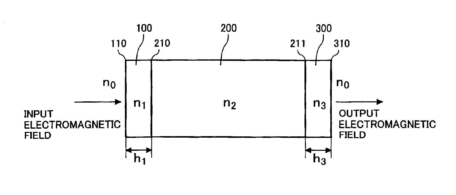
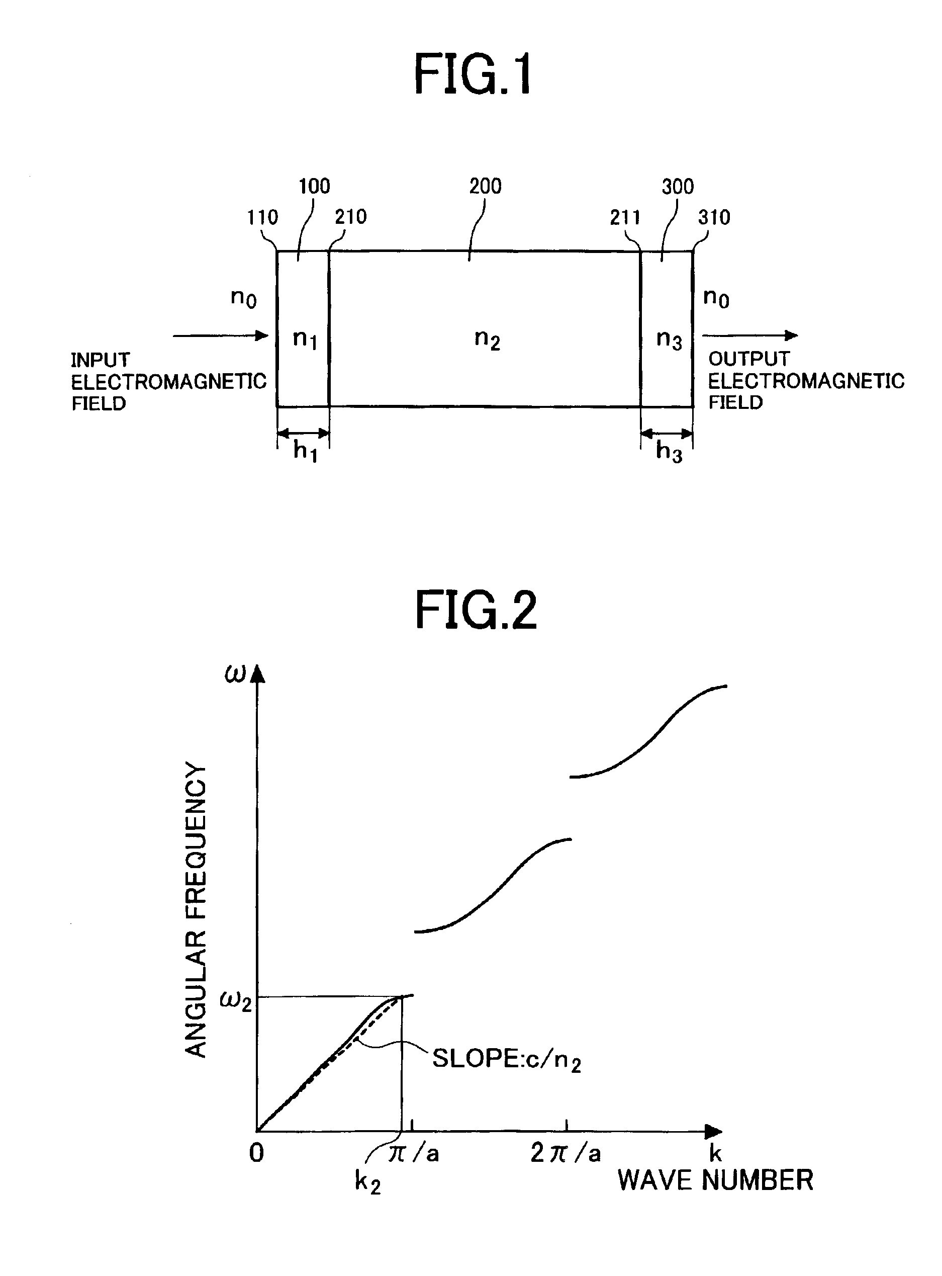
[0036]FIG. 1 is a top view showing a basic configuration of a first embodiment of the invention. FIG. 2 schematically shows propagation characteristics of a photonic crystal 200 transmitting an electromagnetic field.
[0037]In FIG. 2, the horizontal axis “k” indicates the wave number, the vertical axis “ω” indicates angular frequency, and “a” denotes the period of a periodic structure of the photonic crystal. A solid line gives the relation between k and ω when the electromagnetic field is in the photonic crystal. The effective refractive index n2 of the photonic crystal with respect to an electromagnetic field of an angular frequency ω2 is given by an equation ω2=ck2 / n2 using the combination (k2, ω2) in FIG. 2, and the slope of a broken line in FIG. 2 indicates c / n2. “c” indicates velocity of light in vacuum. The characteristics of FIG. 2 largely depend on the structure and material consisting of the photonic crystal.
[0038]In the case where an electromagnetic field having the angular...
second embodiment
[0041]As described above as the conventional technique, in the proposals (for example, Japanese Unexamined Patent Application No. 2000-56146 and U.S. Pat. No. 6,278,105 B1) of the integrated photonic crystal device in which a plurality of photonic crystal devices are disposed on a single substrate, reflection losses on the incident and outgoing sides are not considered. Although the propagation characteristics of the devices in the photonic crystal device group integrated on the single substrate are generally different from each other, the issue of reflection at the connection points is not considered at all.
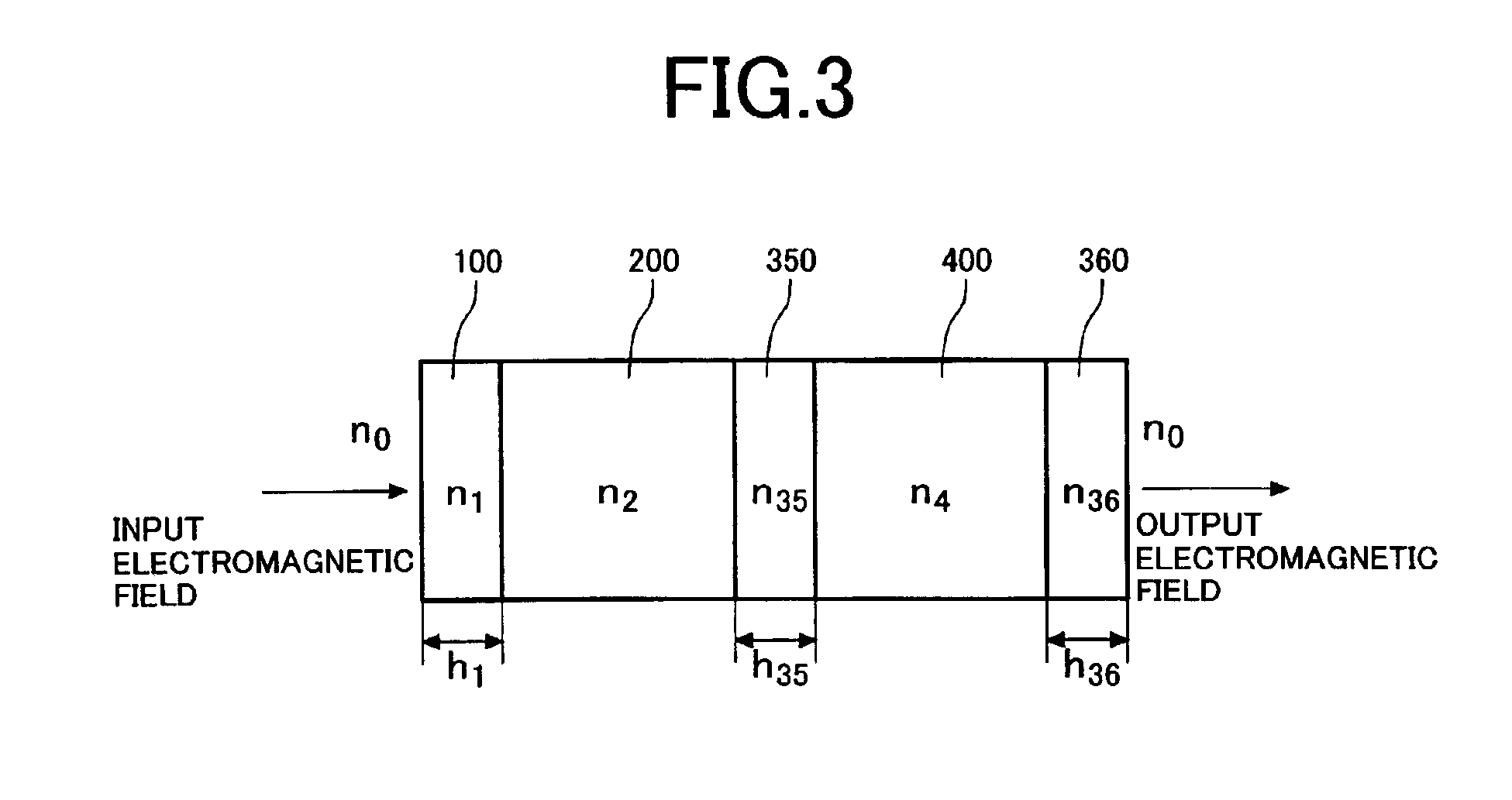
[0042]By employing the present invention, the reflection can be reduced. FIG. 3 shows an embodiment of reducing the reflection. The photonic crystal device includes not only the photonic crystal 200 but also a photonic crystal 400. Since the photonic crystals 200 and 400 generally have propagation characteristics which are different from each other, their effective refractive in...
third embodiment
[0045]In the first embodiment, it has been described that a reflection loss can be reduced by disposing the photonic crystal 100 having the structure different from that of the photonic crystal 200. In practice, the photonic crystal 100 may employ various structures, and the optimum structure also depends on the structure of the photonic crystal 200.
[0046]Therefore, the structure and material of the photonic crystal 100 cannot be uniformly limited. In the third embodiment, an example of the antireflection layer for a line-defect waveguide of a two-dimensional photonic crystal will be described.
[0047]Although an example of a line-defect waveguide of a two-dimensional photonic crystal is described by M. Notomi et al., “Electronics Letters”, Vol. 37, No. 5, pp. 293296 (2001), an action for reducing the reflection loss is not taken. FIGS. 4A and 4B show a structure for reducing the reflection loss for a line-defect waveguide of a two-dimensional photonic crystal. FIG. 4A is a top view a...
PUM
| Property | Measurement | Unit |
|---|---|---|
| Thickness | aaaaa | aaaaa |
| Area | aaaaa | aaaaa |
| Refractive index | aaaaa | aaaaa |
Abstract
Description
Claims
Application Information