

Silicon wafer stage chip scale packaging structure and manufacturing method thereof
A chip-scale packaging, wafer-level technology, applied in semiconductor/solid-state device manufacturing, electrical components, electrical solid-state devices, etc. Size chip packaging requirements and other issues, to reduce the risk of delamination, compensate for warpage deformation, and meet packaging requirements
- Summary
- Abstract
- Description
- Claims
- Application Information
AI Technical Summary
Problems solved by technology
Method used
Image

Examples
Embodiment Construction
[0077] The following describes the implementation of the present invention through specific specific examples, and those skilled in the art can easily understand other advantages and effects of the present invention from the content disclosed in this specification. The present invention can also be implemented or applied through other different specific embodiments, and various details in this specification can also be modified or changed based on different viewpoints and applications without departing from the spirit of the present invention.
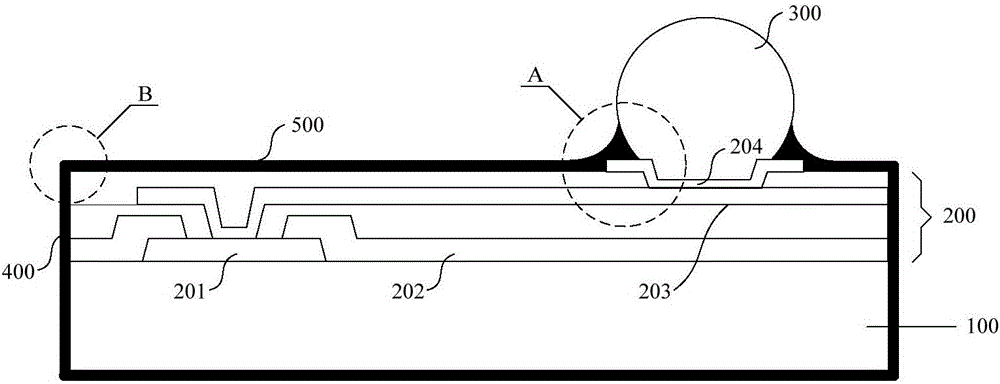
[0078] See figure 1 The first embodiment of the present invention relates to a wafer-level chip-scale packaging structure. It should be noted that the illustrations provided in this embodiment only illustrate the basic idea of the present invention in a schematic way, and the figures only show the components related to the present invention instead of the number, shape, and shape of the components in actual implementation. For size draw...
PUM
 Abstract
Description
Claims
Application Information