Liquid crystal display panel

A liquid crystal display panel and display area technology, which is applied in the direction of instruments, nonlinear optics, optics, etc., can solve the problems of being unable to stop the edge diffusion of the frame glue, uneven diffusion speed resistance, and fluctuations in the edge diffusion of the frame glue, so as to avoid display Poor effect, reduce the risk of liquid crystal puncture, improve the effect of uniformity

Inactive Publication Date: 2017-05-24
XIAMEN TIANMA MICRO ELECTRONICS
View PDF6 Cites 28 Cited by
  • Summary
  • Abstract
  • Description
  • Claims
  • Application Information

AI Technical Summary

Problems solved by technology

[0005] In the production process of the narrow-frame liquid crystal display of the prior art, due to the fluctuation of the amount of glue spit and the uneven diffusion speed resistance, there are fluctuations in the edge diffusion of the frame glue. figure 2 The concave-convex structure shown
When the concave-convex edge of the frame glue 104 contacts with the edge of the liquid crystal 103 to form an inter-embedded shape, the diffusion direction and force distribution of the frame glue are different from the liquid crystal diffusion direction and force distribution, which will lead to different degrees of liquid crystal puncture
[0006] In order to improve the liquid crystal puncture problem caused by the diffusion of the sealant, a barrier wall 142 is added in the non-display area of ​​the CF substrate, such as image 3 As shown, due to the presence of a step difference in the position of the retaining wall 142, the retaining wall is not in contact with the TFT substrate. Therefore, in the actual coating process: the inner edge of part of the frame glue can overlap with the retaining wall, and the edge of the frame glue is neat; however, when the partial When the amount of glue spit out is large, the retaining wall cannot stop the diffusion of the edge of the frame glue, causing part of the frame glue to cross the retaining wall

Method used


Image

  • Liquid crystal display panel
  • Liquid crystal display panel
  • Liquid crystal display panel

Examples


Embodiment

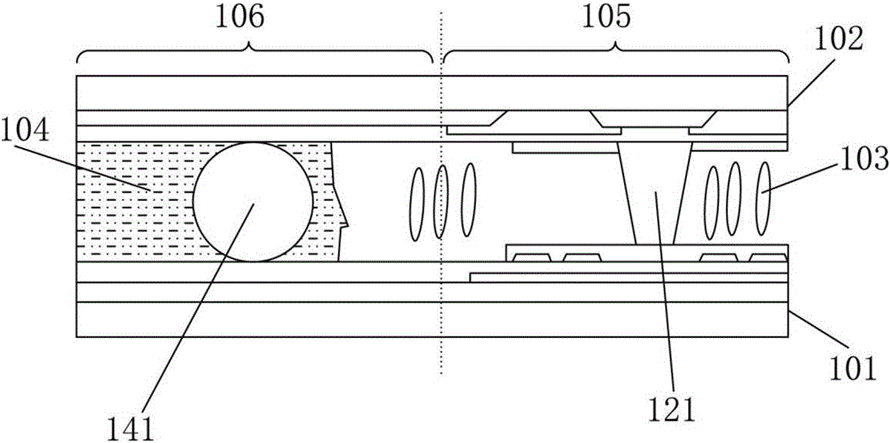
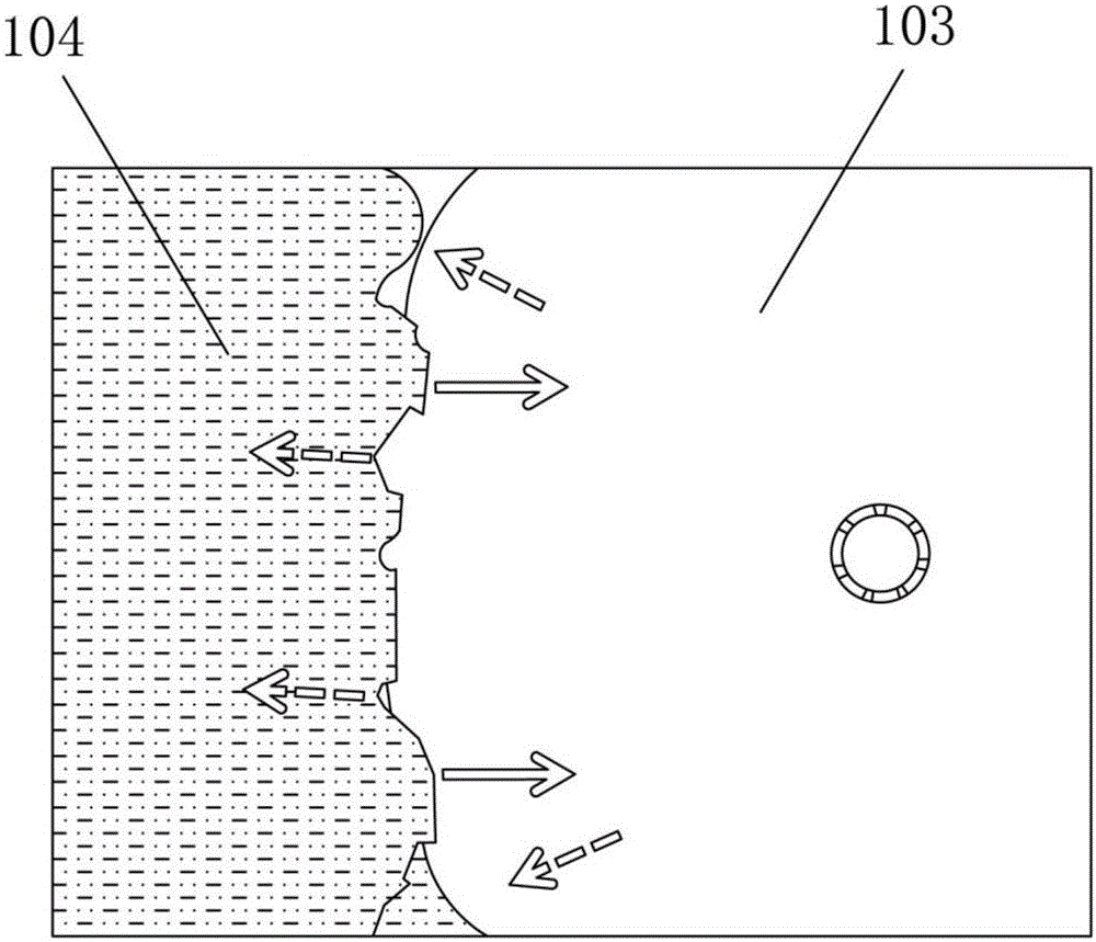
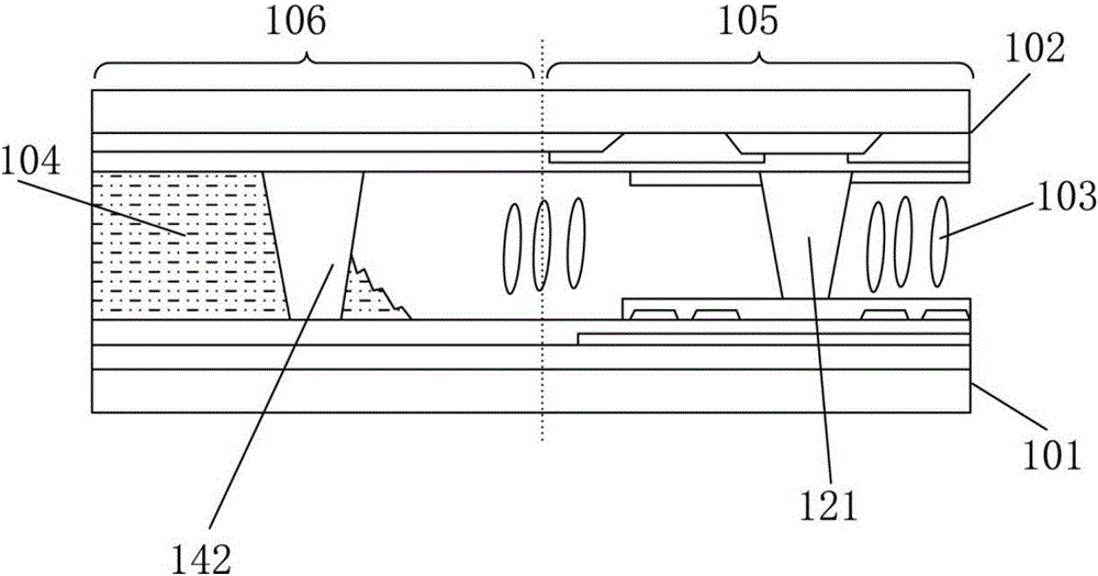
[0057] Such as Figure 4 and Figure 5 as shown, Figure 4 It is a schematic cross-sectional structure diagram of a liquid crystal display panel shown in an embodiment of the present invention; Figure 5 It is a top view of the liquid crystal display panel shown in the embodiment of the present invention to limit the diffusion of the sealant and the puncture of the liquid crystal; the liquid crystal display panel of the present embodiment includes a first substrate 401, a second substrate 402, and a The liquid crystal display panel further includes a display area 403 and a non-display area 404 . The sealant 441 is located in the non-display area 404 and is arranged around the display area 403 . The liquid crystal display panel also includes a first groove 411, a second groove 412, a first spacer 421, and a second spacer 422, the groove wall of the first groove 411 and the groove wall of the second groove 412 A protrusion is formed; wherein, the first groove 411 and the seco...


PUM


Abstract

The invention provides a liquid crystal display panel, comprising a first base plate, a second base plate and a frame glue situated between the first base plate and the second base plate; the liquid crystal display panel further comprises a display zone and a non-display zone; the frame glue is located at a non-display zone and arranged around the display zone; the liquid crystal display panel further comprises a first groove, a second groove, a first spacer and a second spacer; a bulge is formed between the groove wall of the first groove and the groove wall of the second groove, wherein the first groove and the second groove are arranged at one side of the first base place closing to the second base plate; the first groove and the second groove are situated between the frame glue and the display zone; the first groove is arranged between the frame glue and the second groove; the first spacer is extended into the first groove from the second base plate; the second spacer is extended from the second base plate to the bulge and contacted with the bulge. The structure forms a frame glue diffusion buffer layer closing to the frame glue side and a liquid crystal diffusion buffer zone closing to the liquid crystal side; thus the risk of penetration of the frame glue in a narrow side frame to the display zone and liquid crystal puncture is reduced.

Description

technical field [0001] The present invention relates to the technical field of display panels, and more particularly, to a liquid crystal display panel. Background technique [0002] Liquid Crystal Display (LCD)—a flat and ultra-thin display device, is favored by engineers for its advantages of no radiation, lightness and power saving, and is widely used in various information, communication, and consumer electronics products . [0003] The structure of the existing liquid crystal display such as figure 1 As shown, it includes: a TFT substrate 101 , a CF substrate 102 , a liquid crystal 103 , and a sealant 104 . The LCD includes a display area 105 and a non-display area 106, and the sealant 104 is located in the non-display 106 area of ​​the LCD to confine the liquid crystal 103 in the box. The sealant 104 is provided with silicon balls 141 for supporting between the two substrates in the non-display area 106 . A spacer 121 is disposed on the CF substrate 102, and the sp...

Claims


Application Information

Patent Timeline
Patent Type & Authority Applications(China)
IPC IPC(8): G02F1/1339
CPCG02F1/1339G02F1/13394
Inventor 李元行朱绎桦蔡寿金陈国照
Owner XIAMEN TIANMA MICRO ELECTRONICS
Why Eureka
Try Eureka