Hall sensor

A Hall sensor and Hall element technology, which is applied in the field of Hall sensors, can solve the problem that the magnetic offset cannot be eliminated by the offset cancellation circuit, and achieve the effect of reducing the chip size and reducing the cost.

Inactive Publication Date: 2017-05-24
SII SEMICONDUCTOR CORP
View PDF6 Cites 3 Cited by
  • Summary
  • Abstract
  • Description
  • Claims
  • Application Information

AI Technical Summary

Problems solved by technology

Therefore, due to Figure 8 The values ​​of the resistors R1, R2, R3, and R4 in the shown equivalent circuit change depending on the voltage application direction, so there may be cases where the magnetic offset cannot be canceled by the offset cancel circuit

Method used


Image

  • Hall sensor
  • Hall sensor
  • Hall sensor

Examples


Embodiment 1

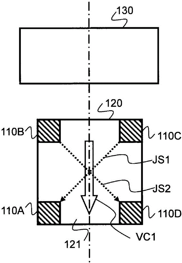
[0053] figure 1It is a plan view showing the Hall sensor of the first embodiment of the present invention. A Hall sensor consists of a Hall element that senses a magnetic field, and a circuit that drives or controls the Hall element.

[0054] First, the shape of the Hall element will be described. Such as figure 1 As shown, the Hall element 120 has a square magnetic induction portion composed of N-type impurity regions 121 and N-type high-concentration impurity regions of the same shape arranged at the vertices of the square magnetic induction portion on the semiconductor substrate. Control current input terminals and Hall voltage output terminals 110A, 110B, 110C, 110D. By making the Hall element 120 of the above-mentioned form, it becomes a symmetrical Hall element.

[0055] Next, the positional relationship between the Hall element and the heat source will be described. A circuit for driving the Hall element 120 is provided on the substrate on which the Hall element ...

Embodiment 2

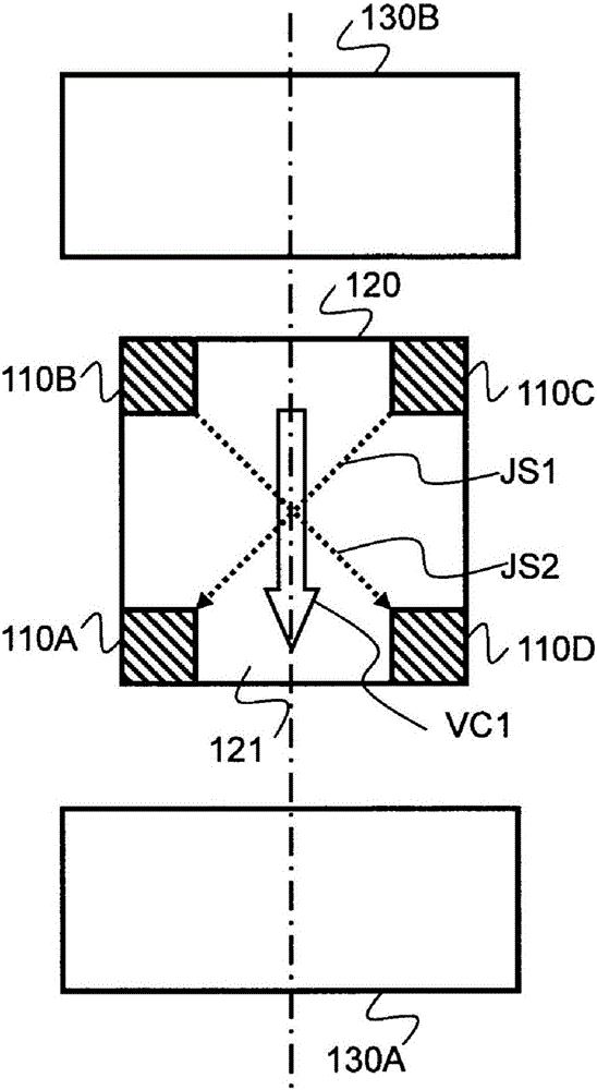
[0072] As a first embodiment, using figure 1 The case where there is one heat source has been described, but the heat generator in the circuit for controlling the Hall element is not limited to one. figure 2 It is a plan view showing the Hall sensor according to the embodiment of the present invention when a plurality of heat generating elements (heat generating sources) 130A, 130B exist in a circuit for controlling the Hall element 120 .

[0073] Even when there are a plurality of heat generating sources, by aligning the center of each heat generating source 130A, 130B on the extension line of the vector sum VC1 of the Hall element control currents JS1 and JS2 in two directions based on the rotating current method, Offset can also be removed.

[0074] Here, the center of the heat source refers to the highest temperature point or region at the peak of the isotherm when the heat source is viewed from above and an isotherm representing a temperature gradient is drawn.

[007...

Embodiment 3

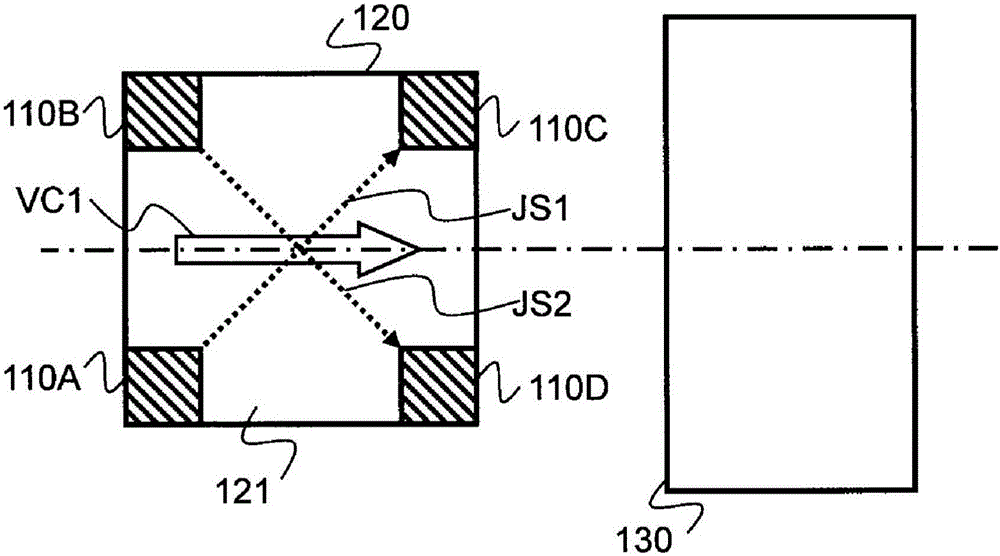
[0077] In addition, as in image 3 shown need to be in with figure 1 and figure 2 When the heat source is arranged in the vertical direction, the Hall element control currents JS1 and JS2 can be controlled by aligning the center of the heat source 130 with the vector of the Hall element control current JS1 and JS2 and the extension line of VC1. to optimize the direction of the , so that the offset can be removed.


PUM


Abstract

Provided is a Hall sensor having an element that, among Hall elements and circuitry for driving semiconductor Hall elements, serves as a heat source, wherein it is possible to eliminate offset voltage with no increase in the chip size. This Hall sensor is characterized in that, in two pairs of elements, a Hall element control current (1) flowing between one of the pairs of elements and a Hall element control current (2) flowing between the other pair of elements interact as vectors, the Hall elements have a linear-symmetric shape in relation to a straight line taken along the vector sum of the Hall element control current (1) and the Hall element control current (2), and the element that serves as the heat source is positioned such that the center of the heat source lies on the straight line taken along the vector sum of the Hall element control current (1) and the Hall element control current (2).

Description

technical field [0001] The present invention relates to a Hall sensor including a semiconductor Hall element and a circuit for driving the semiconductor Hall element, and more particularly to a Hall sensor capable of removing an offset voltage. Background technique [0002] First, the magnetic detection principle of the Hall element will be described. When a magnetic field perpendicular to a current flowing in a substance is applied, an electric field (Hall voltage) is generated in a direction perpendicular to both the current and the magnetic field. The strength of the magnetic field is obtained from the magnitude of the Hall voltage, which is the principle of magnetic detection using the Hall element. [0003] thinking Figure 6 In the case of such a Hall element, when W is the width of the magnetic induction part 1 of the Hall element, L is the length, μ is the electron mobility, Vdd is the applied voltage of the power supply 2 for passing the current, and B is the appli...

Claims


Application Information

Patent Timeline
Patent Type & Authority Applications(China)
IPC IPC(8): G01R33/07H01L43/06
CPCG01R33/075H10N52/101G01R33/07H10N52/00
Inventor 飞冈孝明挽地友生
Owner SII SEMICONDUCTOR CORP
Why Eureka
Try Eureka