
Method of electroplating low internal stress copper deposits on thin film substrates to inhibit warping

A low-stress, thin-film technology, applied in circuits, electrolytic components, electrolytic processes, etc.

Inactive Publication Date: 2017-05-31
ROHM & HAAS ELECTRONICS MATERIALS LLC
View PDF10 Cites 1 Cited by
  • Summary
  • Abstract
  • Description
  • Claims
  • Application Information

AI Technical Summary

Problems solved by technology

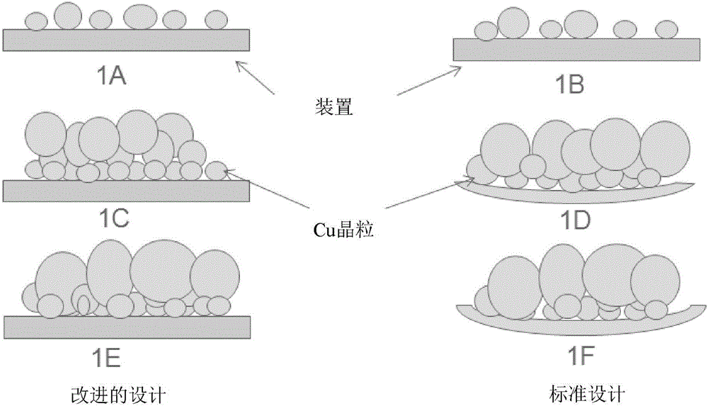
Even many improved copper electroplating baths that deal with internal stress issues when plating on thin substrates have not been able to address warpage

Method used


Image

  • Method of electroplating low internal stress copper deposits on thin film substrates to inhibit warping
  • Method of electroplating low internal stress copper deposits on thin film substrates to inhibit warping
  • Method of electroplating low internal stress copper deposits on thin film substrates to inhibit warping

Examples


example 1

[0057] Prepare the following aqueous acid copper plating bath at room temperature.

[0058] Table 1

[0059]

[0060]

[0061] The components of the copper electroplating baths were made using conventional laboratory procedures in which the organics were added to the water followed by the addition of the inorganic components. Stirring or agitation was performed with application of heat at a temperature below 30°C to ensure that all components were dissolved in water. Allow the bath to come to room temperature prior to copper plating. The pH of the acidic copper electroplating bath is in the range of less than 1 to 1 at room temperature and during copper electroplating.

example 2

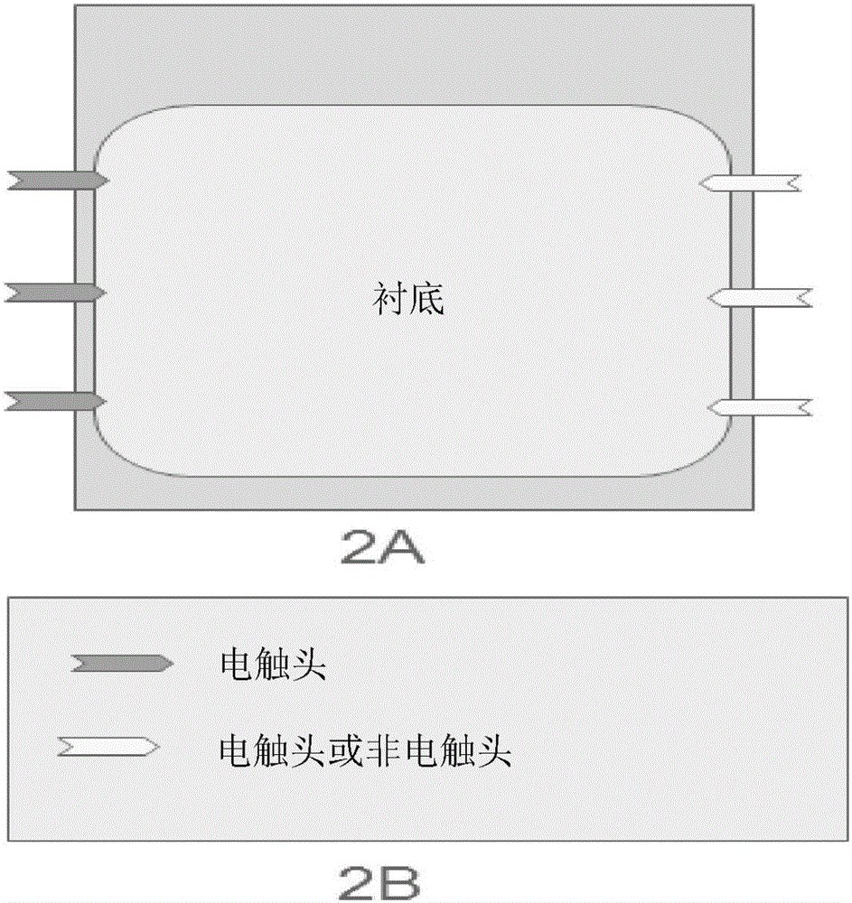
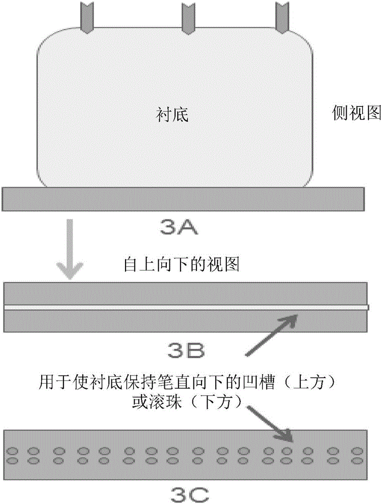
[0063] A plurality of copper thin films having a thickness of 100 μm were bonded to a non-conductive rectangular flat plate plating fixture as shown in FIG. 2A . Each film is secured to the flat plate plating fixture by six electrical contacts, three on each side of the film, or in the alternative by three electrical contacts and three non-electrical contacts, as shown in Figures 2A and 2B shown in . A non-conductive flat plate plating jig with film was secured to a conveyor system, wherein the plating jig was engaged to the conveyor so that it did not move out of a single plane and the conveyor system conveyed the film through a bath containing as in Example 1 1 or bath 2 plating tank. The film remains substantially in one plane during the electroplating process. When the thin copper film bonded to the plate jig enters one of the two copper electroplating baths, the electrical contacts are placed at the potential of a rail that is in electrical contact with the contact poin...

example 3

[0065] Prepare the following aqueous acid copper plating bath at room temperature.

[0066] Table 2

[0067]

[0068]

[0069] The components of the copper electroplating baths were made using conventional laboratory procedures in which the organics were added to the water followed by the addition of the inorganic components. Stirring or agitation was performed with application of heat at a temperature below 30°C to ensure that all components were dissolved in water. Allow the bath to come to room temperature prior to copper plating. The pH of the acidic copper electroplating bath is less than 1 at room temperature and during copper electroplating.


PUM

PropertyMeasurementUnit
thicknessaaaaaaaaaa
elongationaaaaaaaaaa

Abstract

Thin film substrates are electroplated with copper from low internal stress, high ductility acid copper electroplating baths. During the copper electroplating process the thin film substrates can warp or bow. To address the problem of warping or bowing during copper electroplating the thin film substrate is held by a securing means which inhibits the thin film substrate from excessive activity.

Description

technical field [0001] The invention relates to a method for electroplating a low internal stress copper deposit on a thin film substrate to suppress warpage of the thin film substrate. More specifically, the present invention relates to a method for suppressing warpage of a thin film substrate by electroplating a low internal stress copper deposit on a thin film substrate by using a fixing member that suppresses excessive movement of the thin film substrate during copper electroplating. Background technique [0002] Intrinsic or inherent stress in electrodeposited metals is a well known phenomenon caused by defects in the plated crystal structure. After the electroplating process, such defects try to correct themselves, and this induces forces that shrink (tensile strength) or expand (compressive stress) the deposit. This stress and its relief can be problematic. For example, when plating is predominantly on one side of the substrate, it can lead to curling, bowing and wa...

Claims


Application Information

Patent Timeline
Patent Type & Authority Applications(China)
IPC IPC(8): C25D3/38C25D17/06C25D17/00
CPCC25D3/38C25D17/007C25D17/06C25D17/00C25D17/001H01L21/2885C25D7/123H01L21/67288C25D5/04
Inventor Y·H·高L·魏L·戈麦斯M·列斐伏尔
Owner ROHM & HAAS ELECTRONICS MATERIALS LLC
Learn More