Array substrate, manufacturing method thereof and curved surface liquid crystal display panel

An array substrate and substrate technology, applied in nonlinear optics, instruments, optics, etc., can solve problems such as light leakage, dark lines in pixels, etc., and achieve the effect of increasing the aperture ratio

Inactive Publication Date: 2017-05-31
SHENZHEN CHINA STAR OPTOELECTRONICS TECH CO LTD
View PDF4 Cites 11 Cited by
  • Summary
  • Abstract
  • Description
  • Claims
  • Application Information

AI Technical Summary

Problems solved by technology

For curved liquid crystal display panels, because the bending degree of the color filter substrate and the array substrate are inconsistent, the vertical BM on the color filter substrate will deviate from the pixel display area of ​​the array substrate, causing dark lines on one side of the pixel and light leakage on the other side, so black Matrix BM design is not suitable for curved LCD panels

Method used


Image

  • Array substrate, manufacturing method thereof and curved surface liquid crystal display panel
  • Array substrate, manufacturing method thereof and curved surface liquid crystal display panel
  • Array substrate, manufacturing method thereof and curved surface liquid crystal display panel

Examples


Embodiment Construction

[0053] The implementation of the present invention will be described in detail below in conjunction with the accompanying drawings and examples, so as to fully understand and implement the process of how to apply technical means to solve technical problems and achieve technical effects in the present invention. It should be noted that, as long as there is no conflict, each embodiment and each feature in each embodiment of the present invention can be combined with each other, and the formed technical solutions are all within the protection scope of the present invention.

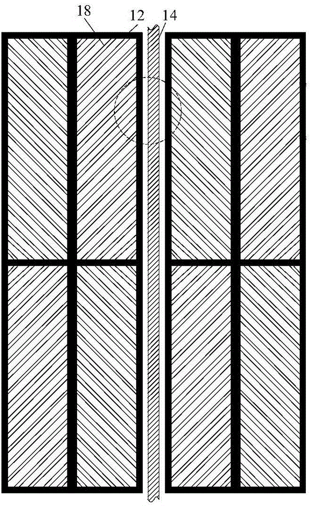
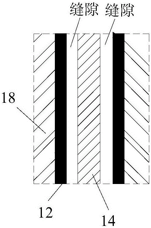
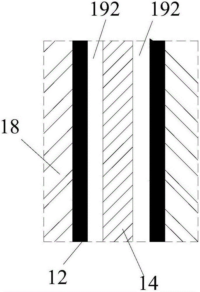
[0054] Such as Figure 2a Shown is a schematic diagram of the planar state of an existing traditional structure LCD. When the green pixel G is turned on and the blue pixel B is turned off, the liquid crystal molecules LC, metal shielding layer SM, and black matrix BM can ensure no blue light leakage. However, when bending the LCD, such as Figure 2b As shown, when the green pixel G is turned on and the blue...


PUM


Abstract

The invention provides an array substrate, a manufacturing method thereof and a curved surface liquid crystal display panel. The array substrate comprises: a substrate, a metal shielding layer arranged on the substrate and comprising a plurality of metal shielding lines, an insulating layer arranged on the metal shielding layer and the exposed substrate, a data line arranged on the insulating layer, a first passivation layer arranged on the data line and the exposed substrate, a color barrier layer arranged on the first passivation layer, a second passivation layer arranged on the color barrier layer, and an ITO layer arranged on the second passivation layer and used for forming a pixel electrode, wherein the metal shielding line close to the data line directly extends to the bottom of the data line to be overlapped with the data line. The array substrate provided by the invention can eliminate light leakage gaps on both sides of the data line, and can also omit a black matrix on the direction of the data line.

Description

technical field [0001] The invention belongs to the technical field of manufacturing liquid crystal display panels, and in particular relates to an array substrate, a manufacturing method, and a curved liquid crystal display panel. Background technique [0002] Such as Figure 1a Shown is a schematic diagram of a pixel structure of an existing conventional array substrate, Figure 1b for Figure 1a A zoomed-in schematic of the local region in the middle. Figure 1b It can be seen that there is usually a distance of 2.5-3.0 um between the metal light-shielding layer SM and the data line DL. The area corresponding to this distance has no metal shading, and there is no ITO electrode to control the liquid crystal molecules, and the backlight will always transmit light after it is turned on. Therefore, generally, a black matrix BM is arranged on the side of the color filter substrate corresponding to the array substrate, and the black matrix BM is used to shield this area, such...

Claims


Application Information

Patent Timeline
Patent Type & Authority Applications(China)
IPC IPC(8): G02F1/1362
CPCG02F1/136204G02F1/136209G02F1/136286G02F1/136222
Inventor 邓竹明
Owner SHENZHEN CHINA STAR OPTOELECTRONICS TECH CO LTD
Why Eureka
Try Eureka